For some weeks, I have been working on a bit serial architecture cpu, loosely inspired by the PDP-8/S.
The plan is to build an experimental pcb, In time for the Open Source Hardware Camp (OSHCAMP) in Hebden Bridge, West Yorkshire, UK at the end of August.
In the last few days, I have read the End of Life notices for the Zilog Z80. This is the end of an era, which for me started in 1978, when I was 13, the Research Machines 380Z, Space Invaders and Lunar Lander.
Unfortunately the PDP-8/S was unbelievably slow. This was partly down to it’s bit serial architecture, and also the slow magnetic core memory.
However, almost 60 years on, we have fast semiconductor SRAM, and fast 74HCxx shift registers.
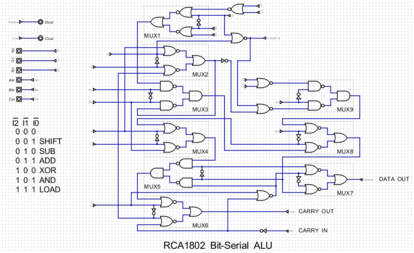
We can create the ALU, the PC, the Memory Address Register and the Memory Buffer Register using modern 74HCxx logic.
As it is a bit-serial architecture - the ALU and combinational logic can easily be placed into a small ROM like the AT28C64 EEPROM.
However - if we choose to use modern SRAM and EEPROM parts - we must use a modern solution to program them.
This is where I deviate from the simple hardware of a TTL computer. I think it is justified to use a modern, low cost microcontroller to program the parallel ROMs and RAM.
In the same week that the Z80 has been canned - I think it should be possible to get Z80 performance from a modern bit serial CPU.
The RCA 1802 also had a 1-bit wide ALU. It took 16 cycles to do most (all? I can’t remember) instructions, so the 8 cycles required to do a 1 byte ALU operation were hidden inside the ALU instructions. It could be clocked at 6.4MHz, which was something like 400,000 instructions per second. The instruction decoding and controls were all logic gates, no ROMs or even PLAs in the chip.
It would be possible to achieve similar performance on a breadboard these days, but clocking much faster than about 8MHz is tough with 74HC because the setup and hold times of the registers start to consume much of each cycle, leaving limited time for useful work.
I’d love to continue chatting about details if you want to go for this.
Yes, the 1801 was a pair of chips: the 40 pin CDP1801U and the 28 pin CDP1801R. The registers are in the R chip while the rest of the processor is in the U. The 1802 merged them into a single chip, though the architecture and instruction set reflected the original design.
Yes. If you look at the die photo you can see that adding even a 4-bit wide, 2-cycle ALU like the Z-80’s would have significantly increased the die size, with presumably bad consequences for chip yield, price, etc. It was a clever choice on their part.
Can you give me a reference (other than CPU Shack) that verifies the 1802 used a bit-serial ALU architecture? Looking at the state waveforms, all ALU operations in the S1 execute state require both a multiplexed high-order latching of the memory address byte, followed by the low order address byte on MA0-7 before the external ram or rom can respond. The waveforms indicate the data from the bus vis the memory gets latched toward the end of the S1 period, which was 8 clock cycles in total. So it would appear the internal ALU logic would have to generate its own self-clocking to take the parallel-latched data from the data bus and shift it 8 times bit by bit to the ALU and back to the D register. It doesn’t appear there’s enough t-states to do this with the normal xtal clock.
A little bit of context to the question - I can’t make the typical propagation delays and SR clocking rates of CMOS from the 70s work to insure an ALU bit-serial micro-sequencer finishes its work by the end of the 8th T-state of the S1 execute phase. This is assuming there is no overlap of fetch and execute operations, which I can’t find any mention of in the RCA literature. I’m also wondering if after latching the byte from memory the ALU did use the fetch period of the next instruction to complete the operation. I can’t find anything about this being the case, but it would be an early form of instruction overlap in microprocessors at that time.
Sorry for the delay. Actually, it’s worse than you say: the User Manual for the CDP1802 COSMAC Microprocessor says the following at the bottom of p.11:
The 8-bit arithmetic-logic unit (ALU in Fig. 2) performs arithmetic and logical operations.
But yes, I think this is marketing hype. You can look at this reverse-engineering of the control circuitry: RCA 1802E - Visual Chips
It says:
The ALU in the bottom left is serial and multiplexer-based. 3 latches above it pick off the lower 3 bits of the internal data bus to select the function. U123 is the main output (goes to D_SHIFT_IN of the datapath), and U63 is the carry out which goes to the carry flag latch U177.
I will have a look at the schematic (image in the linked page) tomorrow and see if I still believe it. But one of the reasons I do believe it is that at this scale, an 8-bit ALU is pretty big. If it existed, it would have to be in the data path (lower right half of the chip). I think most of the circuitry there is accounted for.
Sorry, I can’t help but add one more thing, which (if true) suggests just how much of the description of the chip in the User Manual was not a description of the circuitry. Further down in the reverse engineering of the page I linked, I found:
Notice that this means D cannot be loaded from the databus directly, but each bit must be shifted in via the D_SHIFT_IN input. D is a serial in/out, parallel out right-shifting register.
If true, this means the 1802’s accumulator is actually a serial-input shift register! I had never noticed this. I’ll look at it tomorrow.
The reference I can find is the independent analysis of the 1802 architecture provided by the Visual 6502 Team, from a sample RCA1802 supplied by CPU Shack.
The die was photo-micrographed and then the logic analysed gate by gate from its transistor structure and layout.
The Visual 6502 wiki ceased to be available in 2021 - but the relevant pages have been archived here:
Unfortunately the links to Chuck Bigham’s schematics and analysis of the logic datapath are broken.
Update - the link from the earlier message from Jeff Berkowitz pdxjjb will help a lot - it has the schematic and a lot of the analysis of the underlying logic.
The idea for a computer based on 74HCxx chips arose in 2019, inspired by what, sadly missed, Marcel van Kervinck achieved with his Gigatron TTL Computer a couple of years earlier.
The first prototype Gigatron was assembled on multiple breadboards - and clocked at 6.25MHz - so as to allow 1/4 resolution VGA generation.
I have no desire for colour graphics or sound, and a plain serial output would suffice.
It occurred to me that a lot of what we interface to microcontrollers uses a serial format or serial devices, such as video, audio, disks, SDcards and other peripherals over interfaces such as USB, SPI, I2C and I2S.
Bit serial architectures were in the majority for mainframes up until about 1960, and in electronic calculators until the mid-1970s.
Their demise was really linked to the ever increasing density and number of transistors that could be economically placed on a die.
The 1802 is an anomaly - it started out as a TTL “Home” computer by Joseph Weisbecker in 1970, then converted to CMOS VLSI by 1976.
RCA Designers used a bit serial ALU and universal shift register based accumulator, because it used far fewer transistors than a parallel ALU, yet maintained a fairly rich instruction set - with both shift left and shift right operations.
The bit serial architecture is also extendible - just by extending the main shift registers, and the timing pulse generator. Thus a 16-bit or grater wordlength machine is within reasonable reach, but not so, if a parallel architecture was used.
The other reason for a bit serial architecture is to make it SPI compatible. The contents of the accumulator can be set out to a SPI peripheral - almost as a native I/O instruction.
I have a github repo with more details on in - but it is a work in progress.
Nice! I wish we had the entire 1802 in hneeman/Digital. Of course it would be ridiculously slow. And I’m not quite motivated enough to be the one to do the work.
One of the coolest things about the 1802 is that they provided a guide for reverse engineers literally built into the die. Orient the die photo with Visual6502’s copyright notice at lower right so the register array is at upper right. Then look at the extreme lower left corner. There are two oversize transistors with their contacts labelled: G (gate), D (drain), S (source), SB (source bias, I think) and W (well, I think).
Well Thank You Jeff and Ken both!!!
This is beautiful, die shots plus schematics. So looks like they used some asynchronous design and both edges of a self-generated clock - Ugh. Async design was the last chapter and last lecture of my logic design course at university and was “to be avoided” due to all the hazards. But re serial ALU - there it is, both D and B registers clocked serially.
I guess CMOS on-die delays are a lot shorter than std logic packaged delays, which is usually quoted at 60ns @ 5v.
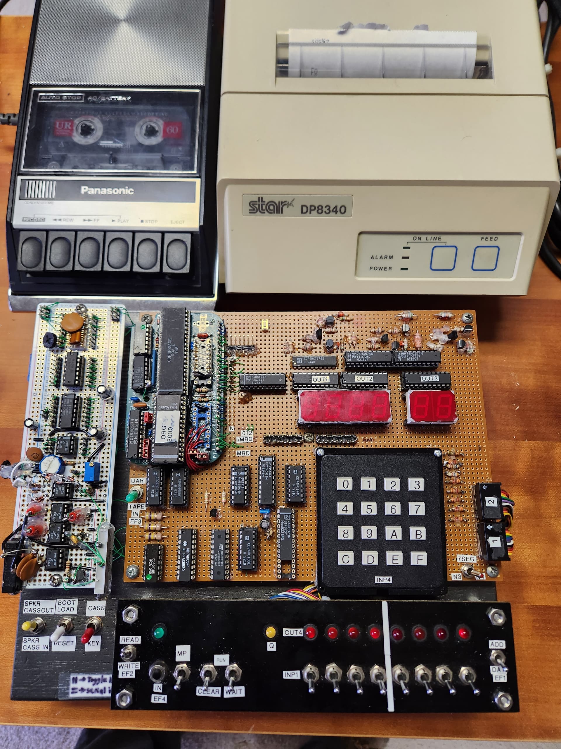
I’ve been having fun with my Cosmac Elf homebrew gone real bad. I started with Lee Hart’s membership card and hacked it rather than start fresh. I cheated a bit by using PIC uc to decode hex for a standard 7-seg display, til311s being very expensive and iffy on the Chinese market. The keypad is also a 1979 cheat using the 74C923.
I’ve also added something that I haven’t seen anyone do using std logic - autoboot clean (no rom) from a cassette using the build-in DMA. I’m sure it isn’t original, but feels more like a minicomputer loading from paper tape (RIM) or DECtape, but no initial toggling required.
I’ve tried to keep everything else '70s era, and consider the HC series OK to use if there was a corresponding LS version. It is very hard to be faithful to the era, Teraterm vs real terminal as exception. I’ve run out of room so time to start afresh and clean everything up!
Oh, that is nice! And I love your “period-appropriate” mindset. In a Discord I frequent, we’re constantly having conversations like “you know, that 128k x 8 flash chip really didn’t exist back then…”
I’m curious: what did you use for RAM? The slowest, oldest, clunkiest static RAMs still in production seem to be 8k x 8, 55ns which maybe became available early 90s (there were 8k x 8 parts in 1982, but they had 150ns access times). So it’s tough to be “period” with RAMs, unless you buy collector’s parts on eBay.
You buy used TIL’s from the UK.(ebay) I like them for logic debuging, and with sockets you just remove them when not needed. I been having problems with
push button switch debouncing and am trying the Logiswitch LS-19P. (6 inputs)
on my next project.
How do you create your cassette tapes?
For my cleaned-up version I’m using (up to) 8K of salvaged 2114s (date stamped '80s, pulled from James T. Kirk’s favorite 6502 computer ). 1MHZ clocked 1802. So definitely not low power, but which makes my '70s date target. I’ve got 2708/16/32 pulls which also are late 70’s. However, I feel like a dirty cheat using a DOS-based programmer. I feel even more uneasy programming using A18, since previously I had hand-assembled my driver routines. But I can’t do anything real serious being that period noble. I considered trying to find RCA’s original tools that ran on IBM or PDPs and using simh, but then realized I’m being a nut case to go this far.