In the final, YT lets us put timed chapters in the video description - so that will help when we get to that point (still a draft so far).
But also - since we lose the row or years at the bottom while zoomed and panned, maybe we could add a “year marker” in one of the corners (that’s always “current” to what the discussion is). Will give it a try and see how it looks.
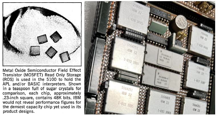
This bipolar technology… I wonder if that’s like what was used in the IBM 5100? I have a 5100 and studied a lot about it, but I’m still not sure how to characterize those “silver can” chips it has. It’s not strictly just TTL based, as some complicated “microprocessor-like” technology was needed to make those silver cans. I came across the notes in the image below, although others have argued that it’s incorrect, and IBM wasn’t using MOSFET tech? (I think those “0.23 in” squares are inside those silver cans {the “IBM 22” chips – and those silver chips are a little over 1" square}, but I don’t yet have a bad card that I’m willing to sacrifice and cut one open to see)
BELOW: my understanding is the two white rectangular chips are the 128 bytes used to store the 4-sets of registers of the system (while the registers are “memory mapped” to main RWS addresses, per the manual and logic diagrams the registers themselves are on the processor card). The silver cans are like a 6KB ROM each - but in this processor card, they also hold the microcode that implements the actual instruction set of the system (to ADD, MOV, XOR, ROR, etc). I’ve no idea what the microcode itself is “written in.” [ but it’s why the 5100 isn’t a huge hot mess of IC like, say, the Datapoint 2200 or Wang systems – yet the 5100 isn’t characterized as a microprocessor based system ]
R0-R15 (16 registers) * 16-bits per register = 256 bits per register file (32 bytes)
4x register files (per interrupt tier) * 32bytes = 128 bytes total
[ so the two “white chip”, each is like 64 byte registers {note: this is my GUESS, I’m not 100% sure} ]
Low power schotty was out by 1974. That Datapoint used SSI TTL and 1970’s tech.
The 74181 came out about 1971. IBM before the PC could spend $$$ on custom chips
because it was all in-house, until the PC.
added Eagle PC reference (have to touch on Eagle!)
minor Tandy 2000 change
added GRiD Compass reference
some font cleanup
year markers still TBD
Upon review, I think I want to add a quick note about the Z-80 SoftCard – it’s significant, as it may have been “the thing” that saved both Microsoft and Apple relative to all the other competitors out there. (or at least certainly helped) Might have to remove the note about the VT52 to do so (which was intended to show how digital had “figured out” 80x24 before any of the Trinity systems – but apparently 40-col was a cost savings thing)
Regarding the very start of this story:
It may be worth pointing out that the CTC (Computer Terminal Corp., later Datapoint) terminals were built around Intel serial shift registers for memory. The Datapoint 2200 (originally) used an Intel serial shift register exclusively produced for CTC, and CTC was founded on this very idea, as incorporated by their very first terminal, the DP 3300. So that Datapoint - Intel connection was there right from the beginning. Or, rather, in the beginning (before there were RAM chips) was the Intel serial shift register.
I had a thought today of instead of a technical narration – we make the video into a song (or a poem)!
I keep adding seconds here and thing, realizing we need more time to cover various aspects. But with a song, we could focus on a few highlights and quickly transition between scenes (and then getting it back to under 10min, maybe even under 5min). But I’ve no experience with lyrics.
Could do both… I mean a “short” and “long” version eventually.
Before TTL became popular, RTL and DTL were commonly used bipolar design styles (with ECL becoming popular at the high end). I²L was pretty unique to Texas Instruments, as far as I can tell. Ken Shirriff explained this technology in his blog post about TI’s 76477 sound chip.
As you pointed out, the 5100’s ROM was made in MOS. But I don’t know what technology was used for the logic chips. The technology was called MST (monolithic system technology) and was introduced in 1968 as the successor to the SLT (solid logic technology) used in the IBM 360. SLT implemented RTL and I couldn’t find out if that changed for MST.
Take #4. Still a couple technical mistakes, but getting close to a final flow.
added some more image inserts [ waiting for an Intellec contact, to include a better interior look ]
added “year” marker boxes at sides (only for the first half, it seemed unnecessary in the second half)
the “IBM guy” is holding an “IBN 5100”; as the Delorean is the time machine of cars, the 5100 is the time machine of computers.\
revised approach in talking about “single board computers”
added Softcard portion (including a humorous quote from Kildall)
creeped time up to13min
NOTE: the reason I mention the core memory patent during the Wang 2200 – is to emphasize how An Wang became successful in the first place: by selling that patent to IBM several years earlier. He definitely knew hardware and electronics. But it’s somewhat distracting, since others might think it is trying to imply the Wang 2200 contain core memory (which it did not).
(I’ve rather clumsily moved a post to a new thread. It feels right to me to allow this thread to remain on the topic of @voidstar’s mural, poster, or video.)
About the Softcard, though I have never seen it mentioned I am pretty sure that those CP/M floppies and manuals with a big Microsoft logo on them are the reason the IBM people thought they were going to Seattle to license a Basic and an OS from Bill. They were very unhappy to learn they had instead to go to California for CP/M.
I had not previously understood the relation between the punch card and the Datapoint machine. This time I noticed that you indicated that the punch card has 12 rows and 80 columns, but the 12 rows in the Datapoint is more likely to be related to half of 24 lines in traditional terminals (sometimes 25 = 24 plus a status line).
You indicated that the PC had 5 ISA slots. Strictly speaking, ISA was the 16 bit slots from the 1984 PC AT. We just called the 8 bit slots “PC slots”. But I think calling it ISA is reasonable for this video.
The term ISA was a reaction to the Microchannel in IBM’s PS/2. They decided to extend the old AT bus to 32 bits calling it EISA (Extended Industry Standard Architecture) and renaming the AT bus as ISA. This is like the HPIB (Hewlett Packard Instrumentation Bus) becoming GPIB or IEEE488 and the Altair bus becoming S100 or IEEE696 so they didn’t have to keep mentioning their competitors when talking about their own products.
Oh, that’s a great point about ISA - yeah I had forgotten about that, the term had come a few years later. I recall the bus approach in the 5150 was “borrowed” from the Datamaster/23 (as was also the keyboard). Other than that, I’m not very familiar with the Datamaster/23 (well, other than it looks quite a bit like the IBM 5120). I’ll have to read through its MIM or manual to see how it refers to its bus design. Oh, or some of IBMs ads from 1981/1982 should have a term listed. Thanks for pointing it out! (or “PC Slot” as you suggest - but you’re right, modern viewers can related to the “ISA” term – anytime I need an 8-bit IBM card, I seach like “8-bit ISA VGA” or “ISA serial” etc)
As for the 80x12, I’ll have to speed-read back through “the” brown Datapoint 2200 book to see if it was mentioned (its where I had recalled it from, but it’s been awhile since I read through that), should be in one of the earlier chapters (sad it doesn’t come with a searchable PDF). I didn’t think 24 row terminals were quite a thing yet in 1970? (maybe more by 1973/4, certainly by digitals VT52 terminal). There were some “weird” word processors and terminals still early maybe 1972, I just didn’t think really any in 1968/1969 that would have influenced CTC? But I’ll read more about it to double check.
On the punch card, I had wanted to put full numbers 1, 10, 20, 30, 40, 50, 60, 70, 80, and numbers on each row (since its confusing that 3 of the rows are at the top of the punch card) but frankly, I just couldn’t get the font quite right and gave up – I think I’d need to do it as another trasparent overlay, and just got a bit lazy there (and just settled on the “80x12” marking).
Is it fair to say the IBM PC bus was “better” than both the S-100 and Apple bus? Everything is subjective and I always appreciate that anything works at all. But what I mean here is, I thought the S-100 required some additional power, making it more expensive or difficult to make third party card? And Apple-bus (not sure what it was called?) had limits on which slots could be used (i.e. not robust where you could just put any expansion into any slot - sometimes making unexpected incompatibilities between combinations of certain cards?).
BTW, a couple chapters earlier, it talked about CTC considering flat panel screens - something about based on some earlier PLATO work, but then something about the resolution just not being acceptable.
I’m guessing what you’ve heard here is that the S-100 bus did not have regulated power, and it is (at least mostly?) true. S-100 bus provided unregulated 8 volts on its power rails, and each individual card provided its own local regulated supply (typically via linear regulators). This was in part because switching supplies for not-quite-homebrew computers weren’t really reasonable at that time, and thus spreading the regulation out over many smaller regulators was more practical. It did mean that S-100 systems tended to run very hot and draw a lot of power, compared to later systems with switching supplies. On the other hand, providing a couple of 7805s on a board was not a huge deal, and I don’t think that would be the fundamental thing that held back the S-100 bus.
A big complaint about S-100 was that the bus was not really a standard bus designed with convenience, reliability, or expandability in mind, but rather a de facto adoption of a bus of convenience. There were many complaints that the signal layout was confusing, inefficient, and often difficult to route, and as the bus grew in popularity and was ported to non-8080 sytems it became clear that it had signal choice limitations. It also did not have a well-defined clock rate, and so compatibility between cards, CPUs, and memory devices was not always guaranteed.
For the most part this was more of a software (and sometimes ROM) limitation than a hardware limitation. There were some slots that had hardware limitations (Slot 0, the Apple //e expansion slot, and the Apple IIgs RAM slot), and boot priority was dependent on slot position (the highest-numbered slots tried to boot first), so in any given system certain slots may have had reasons to dedicate to certain cards for hardware reasons. The big thing, though, is that almost all software expected to find certain cards in certain locations; DOS 3.3 and ProDOS wanted to find disks in slot 6, most communications programs wanted to find the serial port in slot 2, etc. A certain “standard” layout was encouraged by the Microsoft SoftCard documentation, and solidified into hardware design in the integrated card implementations in the IIgs and Mac //e expansion cards.
I guess I didn’t answer the original question, which was whether the PC bus is “better” or not:
I think this is a bit of a difficult question to answer. The PC bus is for a different generation of architecture than the S-100 (8080) or Apple ][ (6502) bus, since it’s for the 16-bit 8088. While the 8088 had an 8-bit external data bus, it was a 16-bit processor that had separate data and I/O spaces, a much larger memory space, and significantly more sophisticated interrupt capabilities, as well as a faster (base) clock rate. (The S-100 bus used faster clocks in some computers, but again, this could be problematic.) This led to a bus with significantly more electrical capabilities, but also a rather more complicated protocol. The PC bus is essentially the 8088 external processor interface, de-multiplexed.
Was it better? Maybe. I think it was “better” in the same sense that the 8088 was “better” than the 8080; it was newer, and thus faster and more capable. It was not necessarily a fundamentally different level of capability, however.
You could make a point that the S-100 bus hat lots of reserve capacity that gave it a lifetime of about 20 years, starting from humble beginnings with a hobbyist computer to eventually integrating entire banks of machines and multi user systems.
(I think, it’s rather amazing that an architecture that came from a kit computer eventually powered such things like trade at the Chicago Mercantile Exchange. – Yes, I just looked up Wikipedia for when S-100 was eventually retired (1994) and found this hopefully truthful fact.)