Help reading EPROM (Intersil IM6654A) and analyze firmware

I now tried another sketch, working better. Simple sketch from site ‘dances with ferretts’.

There were only definitions from data and address lines, so I’ve added the others.
After having fixed the baud setting from the serial output, I got a good dump with correct size.

The output has mainly 11 section of 2 rows of 16 bytes separated by 1 row of FF.
The middle is a bit different. But most bytes are 00.
At 400 octal there’s an ASCII string 032301.#
When converting it with the sixbit BCD character set from an IBM 704 (wikipedia: BCD (character encoding)) it reads

TST / L00010000.

Not sure if the dump is correct, so I want to do it with direct port manipulation.
I only found 2 examples, both with modern EEPROMs.
One puts CE and OE to GND.
The other puts them to D3 and D2. Obviously not Port D, but digital pins 2+3 (at PWM, physical pins 6+7, INT4+5) defined as output.

I don’t have WE but 2x CE. All are active low.
‘E1 must remain high one minimum positive pulse width before the next cycle can begin.’
Maybe that’s the problem.
The truth table is different than usual. I have 4 inputs (including A), a time reference and falling and rising edges.
I don’t know how to set that up (the simplest way) . Obviously handle E1 and E2 differently and not just put to GND.
And again timing questions. Where to use delays and which? Not a delay just while printing the output.
Bipolar PROMs have 4x CE. But I think mine isn’t bipolar.
I did a lot of research and even with help from experts, I wasn’t able to get a proper dump. Each time different results. It’s a very rare edge- or level-sensitive EPROM with built-in address latch and shared address and data lines.
I tried it on several ways with and without Arduino.

I now assume the following:

EPROM is probably defective.

My device is still working without errors, but maybe it’s just the contacts and I think it’s just active for the bus transfer/conversion with either the PLC or the RAM cartridge or both. Due to the location. And there are many 74xx chips nearby, so I don’t assume to have PDP-8 code anyway.

I think, I won’t try it anymore, at least not on my own.

The Retro Chip Tester from the 8bit-museum should now support this chip. Read as 2716 with and without adapter but external definitions, but it’s untested, as nobody owns this chip. I wonder how it should work the same way/pins for the 6654 and 6653 (1024x4 and an additional address line). There is a drawing on the RCT forum.

Maybe I would give my chip away or borrow the Chip Tester. But I think I first try to find someone in my neighborhood with knowledge and a scope.

I now have a dump that should be right.

It was an issue with the breadboard. Another one worked at once.

The ROM contents are strange. No strings (in either encoding) and no PDP-8 code. Values in octal are too high.
Some large sections are 00 and 0F00. Would make sense as a binary pattern. Parts of the EPROM could be defective.

The first 2 bytes are 05 00 hex. Could be the length (500 bytes, 5 lines or 5 words) or a magic bytes header or checksum. Or the start adress of the other 8 ROM code. When I remove that and adding 2 bytes after byte 14, I got a plausible pattern. Most plausible are lines of 16 hex-bytes or 2.

4 lines of 16 bytes starting with 01 03.
Then 2x2 lines 02 00 58 9C 53, rest 00, and one line with 00 each.

05 00
01 03 01 93 02 10 02 10 25 9C 23 40 00 00 00 00
01 03 01 93 02 13 03 93 02 40 00 00 00 00 00 00

02 00 58 9C 53 00 00 00 00 00 00 00 00 00 00 00

The main appearing data starting at 80 (hex) consisting of 2x2 rows and a very similar pattern at 0180.

58 1C 54 5C 56 30 04 33 06 73 04 73 26 3C 24 3C
58 1C 54 5C 56 3C 24 7C 26 3C 24 3C 0F 00 0F 00
18 16 14 56 16 10 08 10 0F 00 0F 00 0F 00 0F 00
18 16 14 56 16 56 19 3C 54 7C 56 3C 54 3C 0F 00

C0-FF all 00
100-17F and 1C0-1FF:
00 00 0F 00 0F 00 0F 00 0F 00 0F 00 0F 00 0F 00

at 0180

58 10 54 50 56 30 04 30 06 70 04 70 0F 00 0F 00

Some of these lines when removing 0f00 have 8 bytes, others 12 bytes.
Does all this make sense to anyone?
The beginning is maybe similar like Intel HEX?
It’s also possible that pins are swapped and contents scrambled.
Or pattern for audio tape. Or discrete CPU.
As there are no strings, it means that they must be in the other 8 ROMs.
So most likely encrypted.

I wouldn’t expect any ordinary industrial device to have any encrypted or even encoded content - it’s a hypothesis, but for me it would be a late one. First things to think of is various ways in which the ROM contents might have appeared out of order: permuted address bits, permuted data bits, even possibly inverted data bus.

But there are many possibilities and I’m not sure what’s a good way of homing in on the right one. You’d be looking either for identifiable code, or strings.

One way to think of strings is as sequences of bytes with the top bit clear but one or two other bits set. That is, look at the bit columns to find runs that look like that. Another possible way is to look for digrams or trigrams - in English that would be TH and THE and so on.

Yes but I haven’t found any strings. Strings could only be the few (German) mnemonics, and the encoding should be one of the sixbit encodings as the device can’t handle ASCII yet.

And concerning the code, almost all PDP-8 codes are valid.
One of the problems is that the order of the 8 ROMs is unknown (due to missing strings).
I tried all plausible combinations.
Please read also my 2 other threads.

Let me just link those for convenience :
Unknown, rare German device, FESTO. Trainer?
Help with c code (bit reversal)

What, if the ROM is more like a paper tape and is loaded similarly into RAM?
DEC had a binary loader format (derived from the TX-0, then used on the PDP-1, and still much alike on the PDP-8), which looked on the PDP-1 (sorry, I haven’t the PDP-8 version ready at the moment) like this:

dio BLOCK_START_ADDRESS
dio BLOCK_END_ADDRESS + 1
... DATA ...
CHECKSUM
dio BLOCK_START_ADDRESS#2
dio BLOCK_END_ADDRESS#2 + 1
... DATA ...
CHECKSUM
...
...
...
dio BLOCK_START_ADDRESS#n
dio BLOCK_END_ADDRESS#n + 1
... DATA ...
CHECKSUM
jmp PRG_START

dio is the instruction for loading a value into the I/O register, jmp is the jump instruction.
There a blocks of data of arbitrary length, with a header consisting of two dio instructions (mind that this is a single-word instruction set with opcode and operand in a single word) with the start and end addresses fo the given block in memory, then the raw data to be loaded into this address range, and finally a checksum. This is either followed by another block or a final jump to execute the loaded program. (The blocks were originally a necessity and artifact of the assembler.)

Maybe this is a (somewhat) similar format?

1 Like

We have to separate this single Intersil ROM and the ROM set of 8 ROMs.

Yes, probably (both) are papertape-like BIN formats (without leader and trailer).
There was a special BIN format with leader/trailer (checksums ?) after each block instead of one at the end like FOCAL69 as mentioned here.

Locations/contents looks more like a RIM format or similar. But then there must also be a RIM loader somewhere and something to tell the CPU to use that (but same for BIN).

Here are all 4 lines starting with 01.

01 03 01 93 02 10 02 10 25 9C 23 40 00 00 00 00
01 03 01 93 02 13 03 93 02 40 00 00 00 00 00 00
01 03 01 01 88 99 80 00 00 00 00 00 00 00 00 00
01 03 01 01 88 99 82 11 03 13 03 93 02 40 00 00

23 40 / 02 40 look like a checksum. I tried both LSB and MSB and also just 40. But the checksums don’t match the data. And line 3 hasn’t even one (or it’s 00).
Also strange the different length. And 93 and 9C are >12 bit.
At the end there’s also no checksum and no jump.
The 8 ROMs just have 12 bit values (PDP-8 code).

It’s also possible, that the strings are in the RAM cartridge, but that is unlikely.
Or that they were at the empty bytes sections. But also rare.

PLCs are very expensive. And especially on the early days where there wasn’t a standard, I could imagine of encryptions.

I now have dumps of all ROMs and I have many details from the manuals, but I can’t find anything in the ROMs.

This would have made some sense, if there were non-German versions and everything was localized.

Another possibility: If I understand you correctly, the strings are used only for the display. Maybe, there are no strings, but there’s just some kind of decoder network for these segments, located in or near the display unit?

Looking for strings could turn out as a major distraction and, maybe, you should look for other recognizable things, like typical loop constructs? (There should also be other reoccurring patterns produced by macros.) Meaning, if you get plausible and senisble code, you probably got it right. (What are the chances of getting this just by random?)

The RAM cartridge also fits in the PLC and there’s also an EPROM cartrige. Non-German versions are also not mentioned in the manual. I found photos and part lists of a cart and there are no hints of EPROMs or labels for a language

The strings aren’t for the display (that can only display F,E,_ and 0-9) but for printout a disassembly.
The display board can’t be easily removed.
Plausible code is hard to find. There are many loops and patterns.

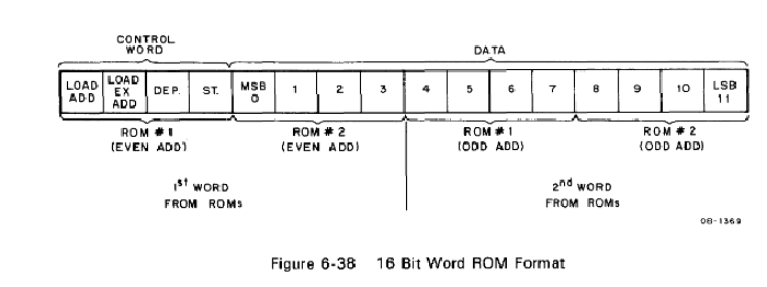
The PDP-8A has ROMs and a 16-Bit Word ROM Format mixing odd and even ROM contents.
4+12 bits, but in fact 4x4 bits.
Similar is the SBC 6120.
Maybe this is also true for my 8 ROMs, and the first nibble is stored elsewhere.
Not sure about address start, autostart and bootstrapping a ROM-less PDP-8.

Taken from bitsavers pdp8a EK-8A0002-MM-002_PDP-8A Users Manual Dec76

Another mystery is the (location) of the 2 empty bytes sections (beginning of ROMs 4+8). Maybe another hint for an encryption. And why do I have 3 RAM chips when I can’t store anything?
ROM 8 can’t be the 1st ROM unless it’s flipped, reversed and/or inverted. Inversion would result in over 12 bit.

Combining all 8 ROMs, I have

3012 bytes, ROMs 1-3
128 bytes FF empty
3968 bytes
128 bytes empty } ROM
896 bytes_________ } 8

dividing by 16 I got (besides 4 bytes, which could be a header and/or checksum)

4 bytes _ 4
188 _________________________ 200
+8 ____ 196 (8=start of ROM 4)

248 _________________________ 256
+8

56 ___________________________ 56 (ROM 8 after empty bytes)

Maybe ROM 8 has to be added or interleaved with ROMs 1-3.

The format is interesting, since it forms a meta instruction, with a 4-bit opcode stitched in front!

Other, I’ve not much interesting to say at the moment. Like @EdS, I’d be somewhat surprised, if the ROMs had been encrypted at that date – this seems to early for such a scheme. (But, as there’s no chance that James Bond and Justin Bieber should be wrong at the same time, never say never [again]. :slight_smile: )

I guess, you have to solve the riddle of ROM 8, in order to get a better overview over the entire architecture. Some “holes” may be explained as assembler artifacts (e.g., where constants or variables were inserted), but if this is a reoccurring scheme, there may be more to it. Maybe, since there’s some empty space left, ROM 8 is more like a configuration file or contains some glue logic?

Strings: It’s possible, that there’s another EPROM, I haven’t found or that there’s just one missing at the empty IC sockets (prepared for ASCII). Maybe they even changed it that the disassembly can only be made by the PLC (which can print comments as well).

ROM 8: If there’s no encryption (and I haven’t found any encryption logic or table), there’s maybe no riddle. Even if the ROM order is not known, I could find patterns or strings even if slightly crossed or flipped or separated. Mainly or only data there like most in the 2nd half.

Intersil ROM: Very few data. Maybe just for configuration or identification.

ROMs 1-8: My device can’t do much. So I assume that major parts of the ROM contents are for “syntax checking”. Although the device can’t execute the Festo instructions, it must know the instructions, check them for allowed operands and put out error codes. Not sure if there’s just a simple syntax check for each line. Maybe there’s even a full emulation with virtual registers and flags. But some checks are only possible with attached PLC like the allowed amount of open brackets.

I think the Festo instruction set with allowed operands must be stored as a table or 2 with error handling.
I described the instructions in the Help with c code thread. 6 digits (1 bit+1 byte+1 word).
In my manual I have tables of the instructions (in fact “functional units”, the real instruction is the byte) and the allowed operations and values.

The functional units are one word. The matrix for allowed operations should be 0-7 but I only found 0-5, so 6 bits. So it’s possible, but unlikely that 2 are packed in 12 bits. Maybe it’s also a mistake.

I’ve searched all my combinations for such tables but without success. So it’s still a mystery how data is stored/packed. All I know is that data (in straight order) is stored as 12 bits LSB.

Codes: There are very few internal functions known in standalone mode. One is calculating a checksum (6 digits for the printout). And there must be a conversion from decimal to octal and an internal RAM check.

I recently re-read the threads to try to get up to speed with where you’ve got to.

You’ve found a CPU, one which runs 12 bit code, and so there must be some ROM somewhere which it boots from. The simplest hypothesis is that all 9 ROMs are in the address space of that CPU. I think perhaps tracing out some bus signals might help.

But that probably leaves us with 2x4 ROMs providing 16 bits and 1 ROM providing 8 bits, and I’m not sure how that would work out. If the single ROM is just data it could probably be read by the 12 bit CPU. All the code would need to be in the 2x4 ROMs.

If you could share the dumped data, here and perhaps elsewhere (VCFed forums?) there may be some people with reverse-engineering skills and interests who could rise to the challenge.

EdS, thanks for your time to read all the posts!
I don’t have equipment for tracing out bus signals.
I don’t assume the single ROM sharing the same address space, the 8 ROMs have 7777 words. It’s on a different board and might interact with the PLC’s CPUs or be for a discrete CPU or the cartridges. I’m not sure if the dump(s) are correct.

It would be great if I could find someone with enough knowledge of (CMOS) PDP-8 and/or PLCs and enough interest and time. He would probably also need all the manuals and that is all very time consuming to scan and then read and check the data. I don’t want to widely share the ROMs to the web. I think the device is very interesting and the (dedicated) code.

The main question is the order of the 8 ROMs. The PLC has 4x2 ROMs not 2x4.
Isn’t it possible to see from the photo how they are ordered?
Or some experience on multi-ROM systems how they are usually ordered?

What about the empty bytes sections (FF)? Could these be bad dumps? I read them multiple times. And the pins are not bent. FF is empty. Same length and position on 2 ROMs. As opcodes invalid.

Also of interest the start address. Is it likely to be at 200 here as well, or at 0. I think it could be hardcoded, I think described in the PDP-8A manual in the 16 Bit format. (I haven’t tried that format as all code is just 12 bit. It’s also the same, I already mentioned as the parse-boot code in the bit reversal thread.) There could also be vectors at 0, 7777 or elsewhere. What is most likely? But as said, I’ve tried it all.

Most similar is the SBC6120. But that has just 2 ROMs, OS8 and different hardware. How does (another) OS/code/bootstrap usually start and look like?

Most plausible is currently the plain 1-8 order (as posted above). Plausible data/patterns at 1000 (octal), 2000 etc. But that is not odd/even merged.

Maybe you’d be OK to share the first 256 bytes of each of the 8 ROMs?

The FF empty bytes are, I would say, almost certainly just unused space. After all, when writing software for ROMs, you can’t go over, so you’re fairly likely to go under. And if they are unused space, I would guess they’d be at the end or the beginning, although that’s not certain.

I would think some words at least must be vectors, and so one might use those vectors to see what byte sequences they point to - surely must be code rather than data. This Intersil 6100 datasheet tells us that the first instruction executed after reset is at octal 7777. So that must be an unconditional branch or jump, and is very likely to be the last byte of two of the ROMs.

Perhaps sharing the last 8 bytes of all 8 ROMs would be useful.

The first 256 bytes are quite long, not sure how I should post them. One long as code tag? 256 Bytes or 256 or 128 words? I already posted them from file 1. As said the first 128 bytes of ROM 4+8 are FF.
The PLC ROMs (I think same CPU) has checksums at 1775-1776, up to 7775-7776. I’m not sure, but I think you have to add +1 to 7777 making it 0.

The last 8 Bytes are 1-8:

2A 30 31 32 10 3C 00 3E
3A 38 04 28 3E 3F 2E 29
28 28 1E 2C 3D 1E 3B 10
3C 1B 0B 0F 03 24 35 00
18 18 18 18 28 1D 04 2F
3F 00 09 3E 2F 2F 1C 1E
0B 0B 19 0B 21 11 2B 28
2F 09 19 20 3A 3F 07 06

JMP J660 -5260
6162 IOT - 6162
ISZ M74 -2074
AND M76 - 0076

CLA CMA CML - 7270
AND I M50 -0450
7677
JMP I J1651 - 5651

JMP J50 -5050 probably data (this line)
DCA I M2654 -3654
SPA SZL OSR HLT -7536
CLA CLL CML -7320

7433
TAD M3717 - 1317
AND M3744 -0344
6500 IOT

DCA M30 -3030 probably data
DCA M30 -3030 "
JMP J35 -5035
AND I M57 -0457

SMA CLA - 7700
TAD M176
JMP I J5757
DCA I M36

TAD M6713 - 1313 probably data
DCA M113 -3113
JMS C121 -4121
JMP J6750 - 5350

JMP I J7711 -5711
DCA M140 -3140
CLA CMA IAC CML 016 -7277
AND I M7706 - 0706

Ah, I see - 6 bits in each ROM. So that must look like it’s for the 6100.

Interesting that the FF bytes are at the beginning, and exactly 128 bytes. Although it looks like the natural scheme for 6100 is to have separate memory and peripheral spaces, I might guess that this could be an I/O window for some peripherals.

Another possibility for them being at the beginning is that the address bus is inverted, and they are actually at the end, in which case the reset PC will be looking at the beginning of the ROM, as we see it.

You mention checksums - how have you been able to determine that something is a checksum?

Edit: just to be clear, you’re saying the very last byte of ROM 1 is 2F?

No they’re lines. The last byte of ROM 1 is 3E. I thought it would be clear as I also added words and opcodes.

Sorry not checksums but date/month and year (according manual). But obviously only true for the PLC ROMs and not mine. I just wanted to tell those locations near the end.

OK, so the way I see it, the last words, taking the ROMs in pairs, would be
3E 29, 10 00, 2F 1E, 28 06
or in binary
11 1110 10 1001, 01 0000 00 0000, 10 1111 01 1110, 10 1000 00 0110
and so in octal grouping
111 110 101 001, 010 000 000 000, 101 111 011 110, 101 000 000 110
or in octal
3651, 2000, 5736, 5006

Unless, of course, the ROM order of the 6 bit bytes is the opposite, in which case
5136, 0020, 3657, 0650

Of all of these, octal 2000 feels most likely to me to be the reset vector, which would presumably (and unsurprisingly) be the start of the ROM area?

Edit: oh wait, if ROMs 4 and 8 both have the padding, then I should have paired the ROMs as 1-5, 2-6, 3-7 and 4-8. In which case, our hex bytes look like this:
3E 2F, 29 1E, 10 28, 00 06
and so in binary
11 1110 10 1111, 10 1001 01 1110, 01 0000 10 1000, 00 0000 00 0110
111 110 101 111, 101 001 011 110, 010 000 101 000, 000 000 000 110
and finally in octal
7657, 5136, 2050, 0006
and now it looks like the 4-8 pair of ROMs have 0006 as the reset vector. If that were right, we’d start disassembling from word 6 of one of the other ROM pairs.

1 Like

Thanks very much!
I think, I’ve checked that combination but didn’t take much attention as I thought this is rather unlikely.

Start disassembling from word 06. Starting from 00. Should I remove words 0-5 or rather skip?
Don’t I need the usual registers like the auto-index registers (at 010-017) or do they move downwards?

I have checked the 3 new combinations , I first got an error, but obviously I missed 1 byte.
I have to continue tomorrow.

So 4-8 is the last pair?

Do I have to check each combination? Could pair 2-6 be the first pair?