First Magnetic Drum Storage (1932)

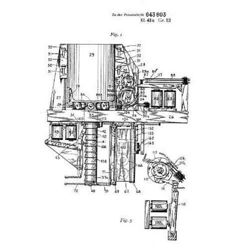
Conformant to a long-lasting tradition of not honoring local engineering feats, I didn’t know that it was an Austrian, who was granted with the patent for the magnetic drum, until I was made aware of this by a tweet by Dag Spicer (senior curator at the CHM). Namely, this was an invention by Gustav Tauschek (1899-1945), while working for an IBM punched card subsidiary in Sömmerda, Germany in 1932.
Also, it’s another example for how computing relied on technology from the pre-computer era, especially when it came to peripheral devices.

For more, see

CHM – 1932: Tauschek patents magnetic drum storage

part of the CHM’s Storage Engine timeline.

One of the most amazing iterations on this was the high-speed drum designed by Ed Fredkin (then at BBN) for the pioneering PDP-1 time-sharing systems developed in parallel at BBN and MIT. As we may all know, accessing core memory involves both a destructive read cycle and a following rewrite cycle. However, Fredkin mused, nothing in this tells you that these have to be connected. What, if we had a drum spinning synchronized with memory cycles and a track length worth the extent of the entire core memory (4K)? Let’s read the data from memory and write it to one track, while rewriting the data from another one – the machine won’t know the difference, while switching context with zero latency. The idea was so convincing that the entire procurement process at MIT was done in half an hour…

(For details see Ed Fredkin’s oral history, pp. 37-39.)

3 Likes

These topics always fascinate me. It always seems somebody says “we don’t have to be stuck doing it this way…” and then bam! innovation happens.

Thanks for sharing this article.

1 Like

Regarding the PDP-1 high-speed drum, it must be said that this was what I personally call a typical Ed Fredkin idea: ingenious, it faces a specific problem with bravado, but it doesn’t scale well – and it had issues. In this case, if you extend the available memory, you’ll have a hard time to come up with a drum for this, and, since the PDP-1 was a low-cost ingenious contraption in its own right, it didn’t have any parity bits or other guards for memory integrity. Thus, if there slipped in any error, it was replicated over and over with no means of detecting this.

(Another “Ed Fredkin idea” was the FRAP assembler for the PDP-1 with its test RAM of just 1K of 18-bit words (which was all the PDP-1 prototype at BBN initially had). Cramming an entire, usable in-memory assembler into 1K is quite a feat, and Ed Fredkin achieved this by the insight that enforcing rules requires instructions. So, less rules = less instructions and less memory usage. FRAP actually stands for Free of Rules Assembler Program. Another important ingredient was to run the paper tape both forth and back, thus packing what would have been two passes into one go. While this was both amazing and ingenious, it didn’t scale well with increasing program lengths for the 4K standard memory and the paper tape — instead of feeding continuously and smoothly as intended — started to chatter in a most annoying fashion, as the buffers didn’t keep up. Which is, at least partly, why MIT started the famous weekend effort to port TX-0 tools to the PDP-1, including the Macro assembler, which became soon standard.)

BTW, Ed Fredkin’s oral history is quite a read — and highly recommended.

2 Likes

The idea of a weekend port, that is something you would not hear of today. What was the typical config of pdp 1 back then?

You really shouldn’t ask me things like this! :slight_smile:
However, here you are:

An important thing to know about the PDP-1 is that it is in it’s essence a commerialized Whirlwind or TX-0 built from transistors-only modules (which had been until then DEC’s bread and butter). There are some architectural differences, like the TX-0 (originating from a test design) has just a 2-bit instruction set and relies heavily on micro-coded instructions, the layout of which varied over time, while the PDP-1 has a 5-bit instruction set (+1 indirection/reverse of condition bit) with additional micro-coded instruction groups (in the 12 address bits). However, all of them followed a distinctive line of realtime computers with a display and sense switches developed at MIT (and DEC’s founders had worked at these projects), and there are considerable similarities in TX-0 instructions and the PDP-1 instruction set, regardless of the differences.

(Another way of looking at this is as a tiny SAGE system in box. Indeed, rumor has it that the reason why DEC developed the PDP-1 in just a 3 and-a-half months effort and announced it in 1959, prematurely to its business plan, was because there were rumors that the Air Force would be looking for such a system for localized missile control. However, I haven’t found any source corroborating this. So this is not a narrative recommended to the serious student. :wink: )

Having said that, the configuration was the first actual production model and had a standard block of 4K 18-bit core memory, a built-in paper tape reader and a separate paper tape punch (also built-in), and a Type 30 CRT display and a light pen.
(More precisely, it was a PDP-1C, as opposed to the production prototypes PDP-1B at BBN and LLNL, and the later timesharing version PDP-1D, which was designed to BBN specifications. For a bit of Internet folklore, the PDP-1D prototype at BBN was eventually used to write and cross-compile the code for the IMPs and was probably the first computer to distribute software updates over the network, as it came online on the ARPANet.)

The machine in question (the “RLE PDP-1”) arrived in fall of 1961 (when that port effort took place), the display only at the end of the year.

Technically, the memory cycle time was 200Hz (or kilo-cycles) and each instruction was 1 memory cycle (5 microseconds), adding an extra cycle, if there was memory access, and another one for each step of indirection. Memory came of blocks of 4K of core memory, expandable in further banks of 4K to up to 64K.
The first few machines didn’t have instructions for multiply and divide, but dedicated shift-step instructions for partial one-bit operations. Eventually, there was a hardware multiply/divide module and machines seem to have come in this configuration as soon as 1962, while older ones were upgraded.

Finally, here’s a link to the basic instruction list.
Not covered here is that the PDP-1 has a rather sophisticated I/O section with direct memory access and asynchronous I/O, an I/O mixer, and a sequence break (interrupt) section, which may account for the better part of the hardware.

(There had been plans for a 24-bit version PDP-2 and a 36-bit PDP-3, which were also mentioned in the 1959 Datamation announcement, but nothing became of those. That is, a single PDP-3 was actually built by SEI and used to process radar cross section data for the Lockheed A-12. This one featured already hardware multiply/divide in 1960, as well as 511 auto-index registers, as seen later on the PDP-8, the memory access time was doubled, though. — SEI is actually CIA’s Scientific Engineering Institute and DEC handing over plans to the CIA, in order to built the machine on their own, must have been quite a show, provided Ken Olsen’s ramblings on government contracts.)
1 Like

Update on the prematurity of the PDP-1’s design, and why there was initially 1K of memory:

Ken Olsen has this version of events in his oral history, which is in obvious contradiction to the story of the rumored Air Force contract, mentioned above, and it it’s a nice little story about a 1K block of core memory (suitable for a 60-page interlude in a Thomas Pynchon novel):

The memory, for many years, was the limiting factor in a computer. We decided to build this PDP-1 a little earlier than we had budgeted because our friends at RCA called us one day and said we have a thousand word memory the customer ordered and doesn’t want. We’ll sell it to you cheap. So we quickly bought it and said, now we’ve got to make our computer. The computer was designed around the thousand word memory. That was the impetus to get going. We sold that 1000 word memory many times. It deserves a place in the museum. We don’t know where it is though because people would buy the machine with a 1000 words. Before they got it delivered they needed more. And they needed eight; four, eight or twelve thousand words. And we’d then sell the machine, that 1000 words over again to someone else.

(Ken Olsen in: https://archive.computerhistory.org/resources/text/olsen_ken/dec.allison.ken_olsen_interview.1988.102630355.pdf, p.42)

1 Like

While the original TX0 did have a two bit opcode, when it was donated to MIT they changed it to 4 bits because most of its 64K words of memory went to the TX2 with only 4KB going to MIT, so fewer address bits were needed in each instruction.

The term “microcoded instruction” meant something completely different for these machines (TX0, PDP-1, PDP-8, etc) than the traditional meaning (which also applied to these machines). It meant that one opcode indicated “operate” which didn’t use the address field of the instruction but instead specified each bit or small group of bits to invoke some operation, such as clear accumulator or rotate the accumulator and so on.

Yes, this is important to note! “Microcoded” means encoding a subset in the operand part. On the PDPs, this also meant that the parent instruction code formed a group of freely combinable instructions encoded as a bit vector in the operand/address part, hence “microcode”. (So you may combine any instructions in the operate group and these will execute in a determined fashion. Or you can combine any skip conditions to form more complex ones.)

Regarding the initial TX-0 instruction set: The initial setup of the TX-0 reminds much of the Memory Test Computer (MTC), a test bed for the core memory stacks for Whirlwind, featuring also a 2-bit instruction set, also built by Ken Olsen.
I’m not sure, if this is really the story, but here is how I understand it – please correct me, if I’m wrong:
Initially, there had been more ambitious plans for a TX-1, but Ken Olsen (and probably others) intervened that these would have been too ambitious, rather build a technology demonstrator first, in order to prove that this fast transistorized architecture was feasible. So this was built, and as it worked, TX-1 was skipped, and the focus shifted to TX-2. Until this point, it would have made some sense to have a MTC-like setup for transistor-like memory cycles, which would prove the reliability of both the basic technology and the memory as well. Notably, this, the MTC, was where Ken Olsen was coming from. But, then, Olsen was also cerncerned by how soon the MTC had been forgotten, so it would have also made sense to provide for future use in the architecture. And, eventually, as the TX-0 went to MIT, it became something different.

As we were speaking of Ed Fredkin, he passed away on June 13.

Compare this Tweet by Dag Spicer:

CHM celebrates the life of computing pioneer, fighter pilot, professor, and businessman Ed Fredkin, who passed away on June 13. Read about his remarkable life in this Computer History Museum oral history (…)

Source: https://twitter.com/dag_spicer/status/1673799376437927936
(The Tweet links to the oral history, already mentioned above. And it’s an amazing (hi)story worth reading!)

For Ed Fredkin on the PDP-1, see this video from Ed Fredkin’s talk at the 30th Anniversary of the DEC PDP-1 Panel (Nov. 29, 1990) @16:20:

1 Like

Ed Rawson and Ken Olsen both worked at Lincoln Labs, and from what I hear they were friends.

1 Like