The PDP-8/S - an exercise in cost reduction

The PDP-8/S was a close cousin of the original PDP-8, but was designed as an exercise in cost reduction - so that a PDP-8 compatible machine could be sold for under $10,000.

In order to achieve this cost reduction, it meant a considerable reduction in the transistor count from about 1500 to 1000 transistors and this required the machine to have a bit serial architecture.

Bit serial was a design technique that was utilised just after WWII notably with the EDSAC. As the memory of the EDSAC was based around ultrasonic delay lines, where the bits were stored as a series of ultrasonic pulses contained within a mercury filled tube, it made absolute sense to make the EDSAC ALU process this data one bit at a time.

The bit serial approach works well for logical operations, because each bit of the operands, can be operated on individually.

The arithmetic operations of addition and multiply, can also be readily broken down into bit serial processes, provided that any carry from each bitwise addition is retained in a flip-flop and re-introduced to the carry input of the full adder for the next bit addition.

The bit serial approach allowed the EDSAC to be constructed using about 3000 vacuum tubes, and provided the only realistic means, at that time, to allow for a long wordsize of 71 bits in the accumulator.

The downside of the bit-serial approach was that the EDSAC machine was slow, returning only about 600 operations per second.

Some 20 years after ESDAC, the PDP-8/S was developed to reduce transistor count, at the expense of execution speed. The PDP-8/S had a 1.33MHz clock, but it took from 48 to 104 clock cycles (36uS to 78uS) to complete an instruction.
As a result, the PDP-8/S was around 20 to 30 times slower that the original PDP-8. However it could run most PDP-8 software including the 4K FOCAL language.

As a result of the bit serial ALU and shift registers used for the principle registers, the PDP-8/S was reported to be implemented in just 519 logic gates.

The reduction in transistor count in the PDP-8/S meant a large reduction in the number of “flip-chip” modules required to implement its logic. Consequently, the PDP-8/S could be housed in a 19" desktop or rack mounted case, rather than the refrigrator sized enclosure of the original PDP-8. The PDP-8/S sold for less than $10,000, compared to $18,500 for the original “Straight-Eight”.

The PDP-8/S was not a big-seller, with between 1000 and 1500 machines sold. It was discontinued after 4 years, because the introduction of TTL used in the PDP-8/I and the PDP-8/L allowed a full spec, sub-$10,000 price to be achieved using the lower cost integrated circuit technology.

Is Bit Serial Still Relevant Today?

The bit serial architecture still makes absolute sense if you want to minimise hardware resources and complexity. One modern example is a 32-bit RISC-V RV-32 core, called SERV implemented using minimum resources as a soft-core (or multi-cores) on an FPGA. A link to a descriptive video is below:

With modern hardware, including FPGA and “Little Logic” TTL gates and flip-flops, we have devices that can be clocked at 200MHz plus. Even if we have to divide this clock by 64, we could still have a 16-bit cpu that could execute instructions at 4MHz or more - equivalent or better to the original IBM PC.

A bit serial cpu makes perfect sense, when so many modern peripheral devices now use serial protocols, especially SPI, I2C and UART interfaces. Bit serial is the principal method for generating monochrome video.

Some years ago, when I first studied the Nand to Tetris (N2T) course, I decided to think about the “Hack” cpu as a bitslice design. Hack is somewhat similar in its accumulator architecture to the PDP-8, albeit 16-bit rather than 12-bit.

The cpu could be implemented as 16 identical pcbs, each of which was constructed from 20, 74xx00, quad dual input NAND gate packages. As 16 of these cards would be needed to create the cpu, we were looking at a total gate count of some 1280 nand gates.

However, by using a bit serial approach, initial investigations suggest that the (nand) gate count could be reduced to approximately 300 gates.

Analysing the logic used in my bitslice, it became apparent that the 2 input XOR, the 2 input mux and the D-type flip-flop accounted for some 90% of the logic.

As you need 4 NANDs to make an XOR, 4 NANDs to make a 2-input mux, and as many as 9 NANDs to make a D-type flip-flop, it makes sense to factor these NANDs out for higher level gates. Alternatively you could use a multi-function or configurable gate.

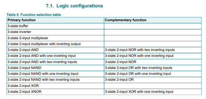
If one was to implement these using the “Little Logic” multi-function, configurable gates such as the 74LVC1G99, (logic configuration in table below) the bitslice could be implemented in about 12 of these devices and 3 of the 74LVC1G74 D-type flip flops. The whole 16-bit Hack design is reduced to 240 “little logic” packages plus a ROM and RAM.

Taking the bit-serial approach, we still need the 12 off 1G99 configurable gates, and we implement the Accumulator, the Memory Buffer and Program Counter register using pairs of 8-bit sfift registers - such as 74HC299, 74HC165 and 74HC595. Add to these about 6 devices for a control unit, ROM and RAM and we have a complete 16-bit TTL cpu into fewer than 30 packages.

Further optimisation might well be possible by reducing the configurable gates into fewer more specialised packages.

The original “Hack” bitslice implemented in 74xx00 nand gates can be viewed on my Github repository here:

4 Likes

Remember the pdp 8 used core memory, the read modify write
was very important part of internal operations. That design looks good.
I was at one time planning to a PDP 8 style machine using CMOS 22v10’s
but decided to go with a different alu model. Ben.

Ben - agreed. The design of any historical cpu was very much dictated by the requirements of its memory sub-system. Approximately 50% of the transistors in a PDP-8 were dedicated to driving it’s core memory.

By the time we got to lower-cost integrated static and dynamic RAM, the 6502 and its contemporaries, especially the Z80 were tailored to the parallel bus and timing requirements of semiconductor RAM.

My recent renaissance of interest for bit serial cpus is to create a minimum hardware cpu that can interface with very cheap SPI RAM, SD Card Flash or non-volatile FRAM.

2 Likes

Before semiconductor memories became practical, long shift registers were used as serial memories. The Kenbak-1 used two Intel 1024 bit shift registers as its main memory, for example.

You can go halfway between serial and parallel implementations. The 16 bit Data General Nova minicomputer, for example, had a 4 bit datapath and took 4 clock cycles to do anything. When the memory is not itself serial, you waste some circuits to convert between the two widths. In an FPGA you can use the fact that two ported block RAMs can have a different width on each port to avoid using normal logic to do the conversion.

The 74181 made a easy alu.When you look at IC prices back then
you can see why the first NOVA was nibble serial. The 74172 made
the NOVA possible. 2x8 dual ported memory, if remember right from the schematic.
About 1975 did mos 5 volt static ram 1024x1 come out, and TTL dropped from $25 to 25 cents for 7400’s. This is something forgotten when one looks at CPU price dropping as the only impact on micro-computers.
The 2901 bit slice makes easy register to register computer alu design, but most designs I have seen use far too complex instruction sets and/or complex micro code.
Why is the 2901 not considered a vaild device for a TTL designed
computer as I can’t think of a Home Brew computer using it?
Back to the PDP-8/S.
When the PDP/8 S was designed cpu speed required for control
tasks did did not need high speed. .1 second seems right for something
pdp 8 might control back then, and a PDP/S fit in well. 110 baud TTY’s
run the same speed or PDP 8/s or Cray.
Only after the 1970’s diid you have the need for faster processing
speed, and thus serial computers tended to be igored as a valid cpu designs.
By the mid 1970’s the home computer proved to be the next market
for computing, thus computers like the PDP 8/S to control things
vanished. The other problem is the PDP/8 stored a subroutine return
address at the start of the subroutine, making a PDP unable to have
code in ROM. Had they left the return address in the AC and had push/pop the AC, the PDP’s (other than 10 or 11) could of had a longer life as a micro computer.

The Z80 actually used a four-bit ALU as well, and used two T-cycles (IIRC ) for the operation itself for any instruction involving an 8-bit ALU operation. (Additional T-cycles would be needed for other parts of the instruction.)

Another place I’ve seen data paths partially seralized is in the National/Panasonic JR-200 where the main 32K RAM was only 4 bits wide and so every instruction doing a fetch from that would take an extra cycle (again IIRC). There was also 2K of video RAM (not special in and of itself, but used for the screen buffer and character set tables) which was a full 8 bits wide.

The Japanese have a very fast version of the Z80.
http://elm-chan.org/docs/dev/kl5c8012_e.html
Not sure if it can be found outside of Japan.

Ken Shirriff has a nice article about this.

One complicated variation was the 68000 which had a 32 bit software architecture but used three 16 bit ALUs. One was normally used for half of the data operation, one for half of the address calculation and the last one could be combined with either of the other two in certain situations for a one clock 32 bit operation. Since 16 bit offsets in address modes were common and operations on bytes and 16 bits were also common this was a very reasonable trade-off.

1 Like

Yes - I encountered the Kenbak some years ago, and have recently been reading up on it - as it is a valuable example of a bit serial machine.

There is a list of original documentation available from the link below, when a reproduction kit was offered several years ago:

http://www.kenbakkit.com/

In 1987, the Kenbak-1 was judged in 1987 by the Boston Computer Museum to be the first commercially available personal computer. Sadly, because of pricing ($750) and poor marketing, the venture failed with only 40 to 50 machines sold. This makes them very rare with only 14 known examples remaining.

The comprehensive reference manual has a detailed description of the design including timing diagrams, circuit schematics and list of ICs.

http://www.kenbakkit.com/manuals/KENBAK-Theory_of_Operation-07-Release1-Searchable.pdf

John Blankenbaker (now 90) the creator of the Kenbak-1 appears in this VCF East video - performing some maintenance on a rare example of his machine:

The Kenbak-1 had a capable instruction set - sufficient for the user to experience the basics of a considerably more expensive minicomputer.

http://www.kenbakkit.com/manuals/KENBAK-Programming_Reference-07-Release1-Searchable.pdf

Originally it was intended that there would be an optional punched card reader fitted - and the slot for this can clearly be seen on the top right of the front panel. Sadly this feature was never implemented.

The memory was limited to 256 bytes implemented as two 1024 bit Intel 1404 shift registers. This seems the overall limitation of the machine in that the cpu had no provision to address a larger memory space.

It is interesting to note that a contemporary of the Kenbak was the CTC Datapoint 2200 - another bit serial TTL design based initially (Version 1) on shift register memory and then subsequently on Intel static RAMs.

https://oldcomputers.net/datapoint-2200.html

The ISA of the Datapoint 2200 was shared with Intel and Texas Instruments, as CTC was looking for a more integrated solution from a mojor IC manufacturer - allowing a considerable reduction in chip count and cost.

This gave rise to two new microprocessor designs - the Intel 1201 (later released commercially as the Intel 8008), and the never released TI. TMX1795.

CTC were disappointed with both the Intel and TI offerings describing them as slow and with reliability problems “too little, too late” and continued with custom TTL processors right up until the early 1980s.

The 1201 / 8008 architecture was 8-bit parallel and included the familiar A,B,C,D,E,H,L register configuration, which perpetuated through the 8080, 8085, Z80 and arguably influenced the x86 family.

1 Like

I own a 1971 Datapoint 2200. Do you know of anyone who would be interested?

2 Likes

The Educ-8 was also another bit serial computer - EDUC-8 - Wikipedia

hi, it is still available?

The EDUC-8 plans are online but you have to dig for them.
Parts may be harder to find. And hiding a PI in empty case
does not count as REAL EDUC-8, or Kenbak-1 or PDP-8S.

1 Like