Down do 256nS by just using Register writes for GPIO toggles… 200nS to go!
Down do 256nS by just using Register writes for GPIO toggles… 200nS to go!
Taking this off on a slight tangent…
Some ~30 years back I interfaced a modern computer for the day (A BBC Micro) to my older CPU system - a Sinclair Mk14. Those who know the Mk14 will think the keys on a ZX80 were brilliant by comparison… Hence my desire to interface it. It worked well - I wrote a little assembler on the Beeb for it, and I could download code into it.
Sadly my beeb was stolen, however I still have the Mk14 - phew ![]()
And in recent times, it’s been done with a Raspberry Pi too Old Meets New - Raspberry Pi Forums that thread was started some years back, but has been recently updated.
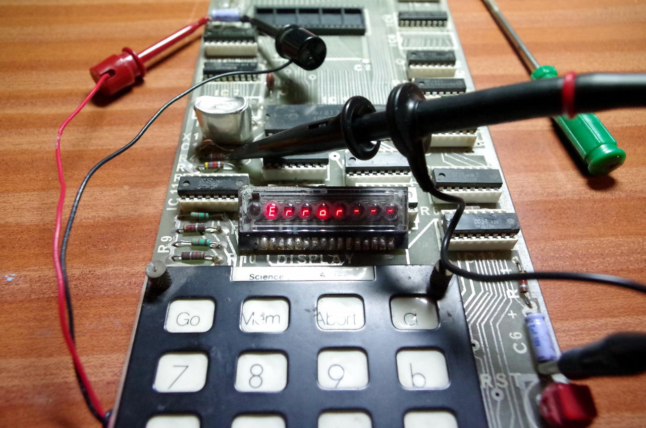
My Mk14:
It might need some TLC…
-Gordon
The timing is tight … I have to do alot of work to make an ESP32 work consistently.
my next CPU is the BeagleBone Black. It has 2 Programmable Realtime Units that have a 5ns per instruction timing and a 1 instruction/clock cycle. The Caveat is the bootup time - and Amiga will be spinning its wheels for what it feels like is a month before the BeagleBone is fully linux booted.
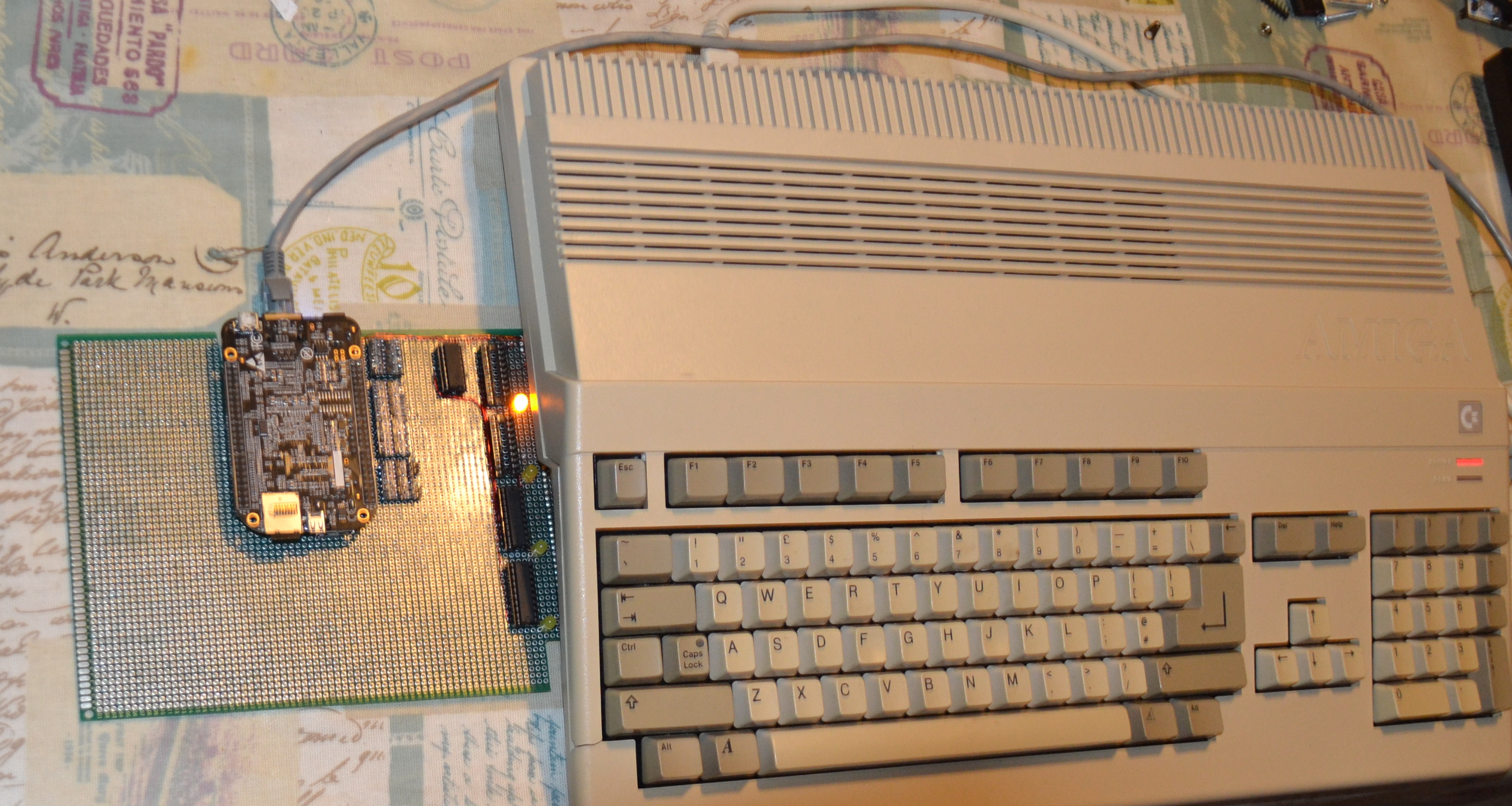
Just a thought but would it work for the microcontroller to fill an SRAM with code then let the Amiga run?
I am doing something similar with an ESP32 and a modern recreation of the Sinclair QL I am working on (68SEC000 at 7.5MHz).
I have found it easier to simply put the ESP32 behind some dual port RAM in the IO area. It just runs a continuous loop updating the real time clock, uses a PWM output to run the fast interrupt timer, and all keyboard input is handled through a single byte register.
Luckily, small dual port SRAM is quite reasonable in price, and simplifies the design greatly.
I did look at dual port RAM, but in this case the Amiga Clock is on a 4 bit bus with only 4 bit data lines attached. (for BCD type data) - I want to create a pseudo serial where I can read the same address multiple times and the ‘Modern CPU’ on the other side increments the meory location.
Much like I2C memory where you write a command and address, and then you burst read/write and the device handles the smarts of incrementing the memory location.
@Dave - I am interested in your QL project … having owned one in the early 90’s. it unfortunately was thrown away when the microdrive broke and I couldnt play chess anymore.
So, how would you manifest this. Is the data “clocked” in via, say, Chip Select logic that isolated the magic byte?
That is you have your MCU wired up to your CPU, then you have, what, the R/W lines, Address lines (however few there are), and the Data Bus lines from the CPU. Then you’d have a separate Chip Select signal from the address decode logic.
I’m just visualizing that the CS signal acts as an ad hoc Clock Signal to clock in (or out) the data. Because once you do your MOV DEST ← SRC instruction, where DEST is your magic address, the data bus will have the SRC data on it, the address bus will have your DEST address on it, R/W will be Write, and the decode logic will set CS HIGH (we’ll say).
A cycle or so later, the CS will be low, because the address bus has moved on to the next instruction, thus dropping CS.
You MCU can use CS and R/W (and the address bus) to react appropriately, it just has to act fast enough before CS goes away, and the data bus moves on. It’s one thing to latch the data on a CS toggle so the MCU can read it “at it’s leisure”, but quite another for providing data back – that data has to be on the data bus really soon after CS goes high I imagine (I imagine CS is one of the last signals in the process).
But, in the end, it seems that the CS signal is the toggle to get work done. Save that you have to do everything within the clock life of the CPU, since it’s not going to wait.
My scheme (unimplemented) has 7 control signals, and 8 data bits, designed to be used off of GPIO ports, rather than the Address/Data bus of the CPU. An async protocol relying on handshakes. A “Get It, Got It, Good” system. My hope is to use it in a 4MHz system.
Things like, set WRITE to HIGH, put the data on the bus, set HOST DATA READY to HIGH. Co processor sees the WRITE HIGH, and the HDR HIGH, reads the data, asserts COP DATA READY. Host sees that, de-asserts HDR, Co proc sees that and de-asserts CDR. 1 byte written. If either the host or co processor stalls, they just wait for the handshakes.
On the Bus I have 4 ADDR and 4 DATA lines with a RD/WR and CS line…
I wanted to use the RD line as the clocking mechanism. The RTC has 16 addresses that give out BCD data on the date/time in the clock.
I want to re-purpose a address and use it as part of the protocol. Wire F to address 16, the MCU can detect that and then do some smarts on what happens next.
e.g. Write 0xF 0x0 … selects bank 0
then a READ 0xF will return the byte contents of bank 0… after every RD strobe, the memory address in the MCU is incremented… and after every read the next nibble is placed on the bus.
Richard
I added some profiling of the STM32 F4 processor - its small and supposed to run at 80Mhz. From my experiments it can only toggle a pin at 1.4Mhz rate (300nSecond per pulse). As a software interface, it doesnt look like there is enough headroom to watch the bus - and do other things
From the charts, the BeagleBone PRU looks like it can do the task
The BeagleBone and its PRUs are exactly what the UniBone interface to the PDP-11 UNIBUS (discussed in this previous post) use, apparently with meaningful success. The author of that project has emulated several peripherals, including disk drives and RAM.
I have got some distance in the prototype… The interface and all the logic level converters are running. I have the high byte address wired in and now to program the PRU on the Beaglebone. The address MUX is running - so now just to start debugging…
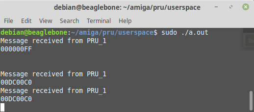
Got some action… although its same excitement level when I tell my partner that I got a LED to blink 
High and low address decode is working - I manage to intercept the memory bus reading the RTC address. Although nothing is there yet, its a good promise. 0x DCxxxx are all for a clock! … tons of wasted address spaces.
Congratulations! Partial address decoding is a good trick - it’s not wasteful, until you find you’re out of addresses. And then you can adjust your tactics.
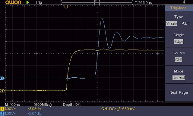
I have had to revise quite alot; the logic level converters are a source of pain and lots of noise, of which that noise was being sent down the power rails. A ton of decoupling has been added and next I going to try other level shifting methods. I have added to my blog of trials and tribulations.
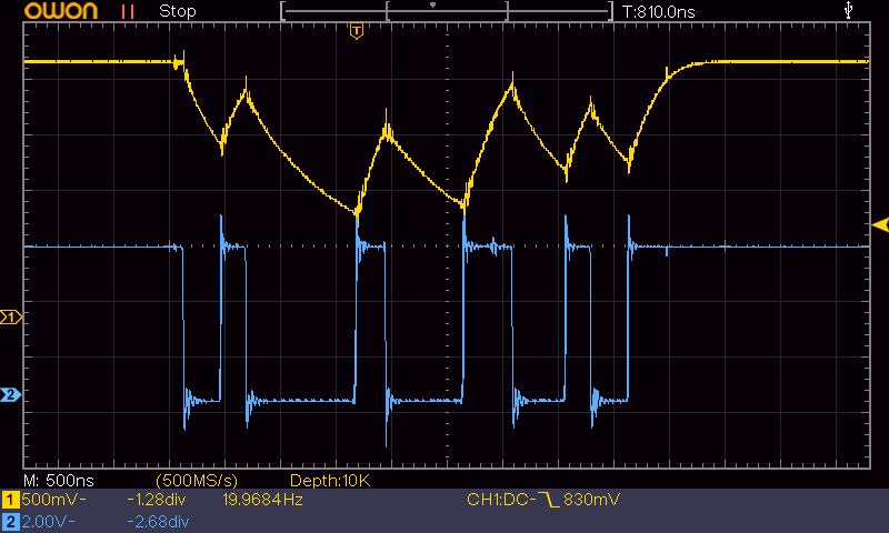
Findings : Using a Zener clamp for level shifting resulted in a failure… or a success in learning. (I prefer the latter) - The generic 3v3 Zeners just cant do the speeds - also adding a ton of capacitance.
Yellow trace is output to Beaglebone… Cyan is 5V logic input…
Wow, I knew Zener diodes added a lot of capacitance, but that’s wild.
A change of tact…
redesigning to use 74LVX conponents on the bus interface with standard 3.3V logic on the board only. I was hoping to use 5V until the final stages… but it doesn’t seem like a good idea anymore 
74LVX244 for the address inputs and 74LVX245 for the bidirectional data bus.
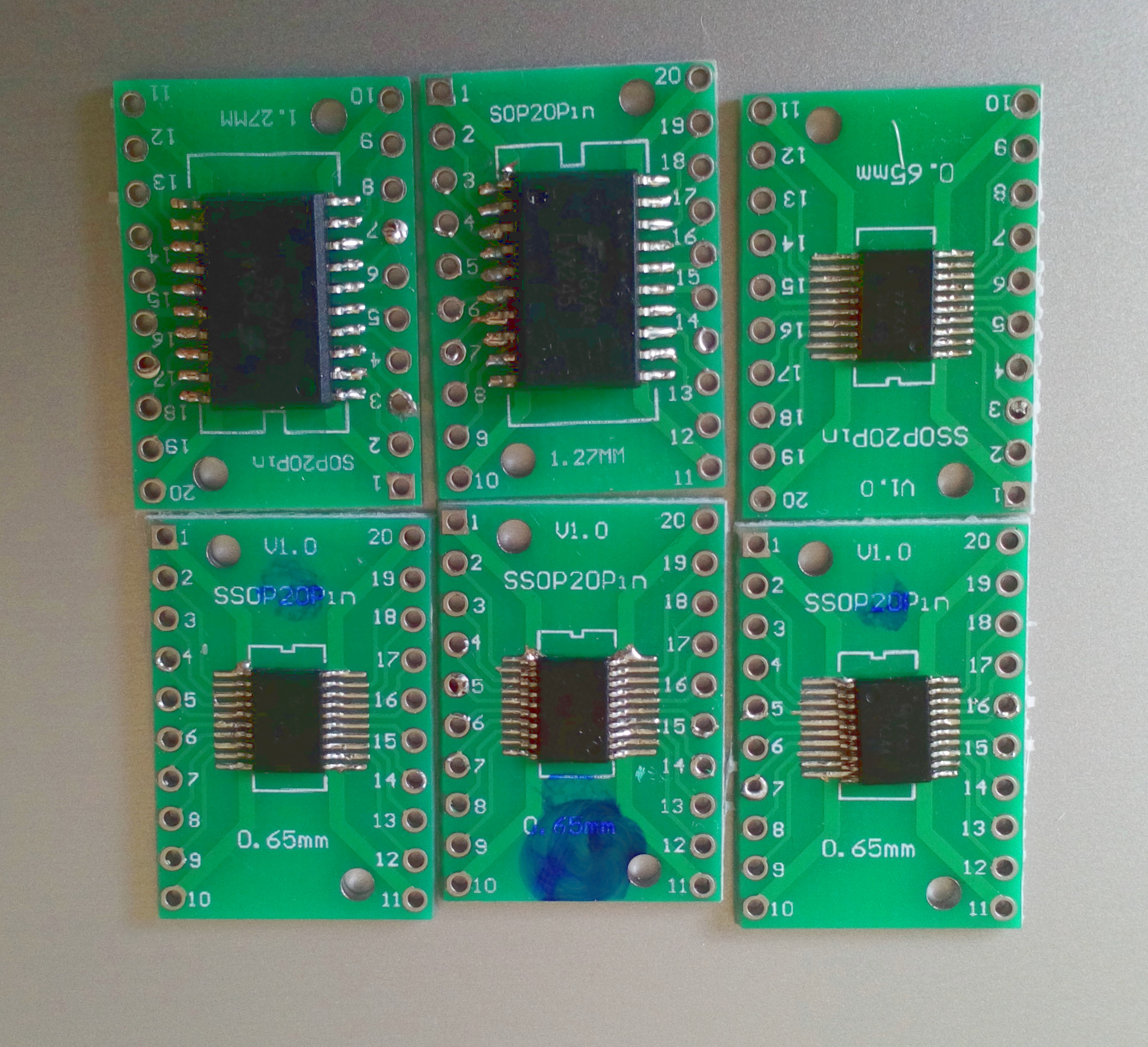
Soldered the new arrivals… wow they were a pain… there was one casualty… and one soldered backwards… (ho hum)
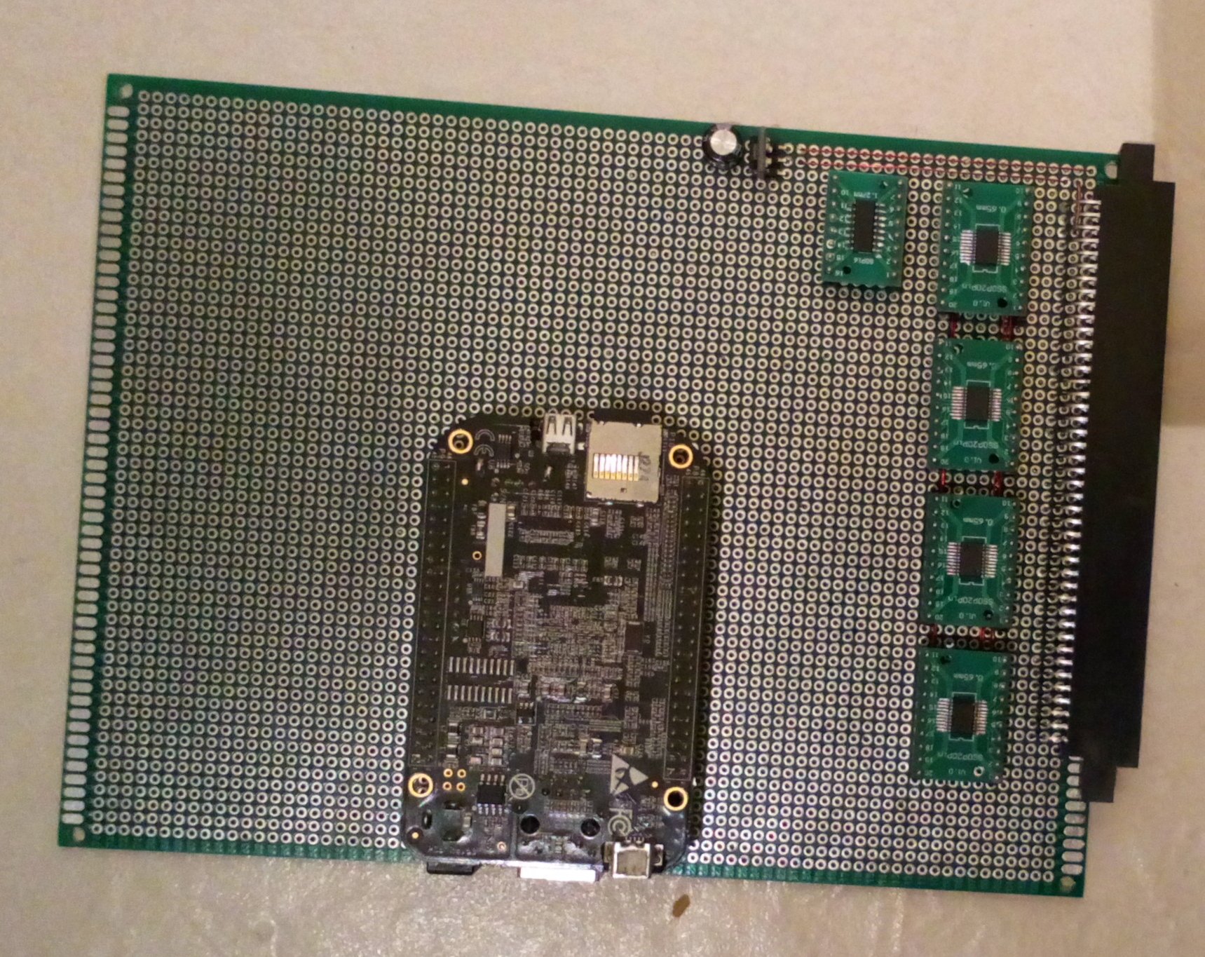
Got the 245 and 244’s on adapters.
Version 2 of the prototype taking shape… All 3.3V logic and annoyingly small packages
The 4 muxed control/Data lines… One for RW/AE/LDS/UDS and the other 3 are Address lines 0…23
the 74xx137 is a 3-to-8-Decoder so I can use 4 lines and select one of the OE lines on the 74xx244 inputs.
Using the 74LVX244 as they have level shifters built in.