Very nice article with great research and lots of juicy links - well done and many thanks!
A bit of a surprise to me to learn that Calma’s first generation GDS was already available for use in the 6502 layout - there was a GDSI system at my first place of work as late as 1984/5, but the GDSII system was the one I got to use. (GDSII is still, today, the file format of choice to ship chip layouts to mask making.)
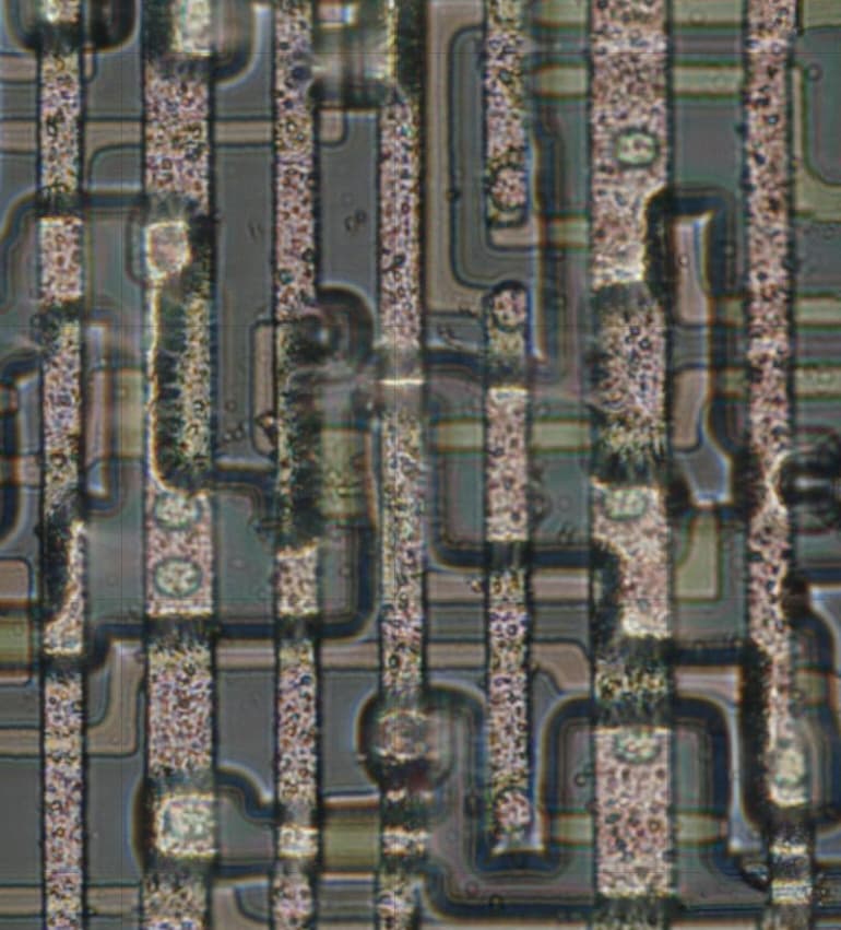
In this bit you identify a particular NOR gate in the ALU:
The transistor at the output of a gate is a depletion-mode pull-up, with the others as enhancement-mode transistor inputs — so, for example, the NOR gate with transistors AA and Y as inputs had gate widths of 0.7 mil and length of 0.35 mil, and a depletion-mode pull-up of 0.3 mil width and 0.8 mil length. (In theory, someone could double-check this against Antoine Bercovici’s die photos of the 6502 rev A, by locating individual transistors and trying to find the corresponding transistors on the logic diagram… I have not, and leave this as an exercise for the industrious reader.)
Here’s the NOR gate in question in Visual6502 (there are 8 of them in total) - and here it is (rotated!) in the siliconpr0n slippy map:
Nice detail on the T and B (Top and Bottom) inputs of a NAND stack. The B input switches the transistor that’s closest to the rail, has more capacitance to switch, and is the slower input. As such, the latest-arriving input should be connected to the faster input, to minimise the overall output delay.
I feel a need to paste a few slides from Bill Mensch’s presentation on his working life:

I did laugh at Motorola proclaiming themselves as a Ponderous Pachyderm!
Thanks for the feedback!
That is insane how you were able to find the mystery transistor… I still don’t get how quickly you were able to do that — aside from starting with Visual6502; I hadn’t thought of going through that. (I don’t have the “zen” of looking at these layouts; I can just barely visualize the individual transistors as transistors instead of pretty lines and things.)
They had it for the 6800 at Motorola as well.
According to Harry Bawcom, Motorola had a higher-end setup:
The Calma operator converted the drawings done on a plastic with a matte surface, called stabilene, (paper was not dimensionally stable enough) to a set of coordinates that was saved on punch cards. The punch cards were then used to drive the rubylith cutter. I did not witness this process at MOS Technology. Motorola was more advanced and did not use punch cards. The coordinate file went directly to the rubylith cutter and that I did see.
I wasn’t able to confirm about the punch cards — Bill Mensch didn’t remember it — so did not include that detail in my article.
Ken Tindall referred me to this 1978 BBC documentary that included a really cool video of someone doing the digitization for Intel (at around 07:50); I might edit to add the video under “further reading.”
p.s. let me know if you have any questions… I’ve been in contact with most of the remaining team members, and they’re not getting any younger, so if there’s anything technical you want to know, now’s the time to ask ![]()