This post (to be thread?) is an outline of how I came to build a TMS 9900 homebrew computer on my desk at work (I work at university, teaching Computer Science), and what casual digital retrocomputing homebrew can look like in the current era. I previously wrote up some information about the TMS 9900 platform itself on this forum, for those who are interested.
Some time in late 2019 or early 2020, I decided to build a TMS 9900 homebrew computer, but I didn’t move on it immediately, and Spring of 2020 my work was forced online and I took up residence in my basement, further cluttering my work space, putting the idea on pause. Eventually, however, I ordered parts on eBay, and started work. I think the impetus to stop thinking about it and actually order was a discussion with @EdS on this very forum, although I couldn’t find the particular message.
I have been doing my work using mostly period-appropriate equipment, although some equipment that would have been out of the price range of a homebrewer at the time. That includes:
- Solderless breadboards
- A bench DMM
- An HP 1630G logic analyzer (this would have sold new for tens of thousands of dollars in the early 1980s, but a significant portion of my purchase price was shipping and handling!)
- A Tektronix 60 MHz analog 2-channel 'scope
- A Tektronix 100 MHz analog 4-channel 'scope
- A Tektronix 100 MHz analog / 100 MSPS digital storage 'scope (I believe this was released in the late 1980s, so probably anachronistic, and also certainly out of the hobbyist’s price range at the time!)
By early July of 2020, I had built up the basic requirements for a TMS 9900 system on a breadboard, including an oscillator, four-phase clock generator, and reset logic. I took some time to learn my equipment, some of which I had had on the shelf for a while, but not really had a chance to use in anger. One of those pieces of equipment was the HP 1630G Logic Analyzer, a 65-channel 25 MHz standalone logic analyzer.

Here is the analyzer viewing the 12 MHz input and 3 MHz four-phase output of the TIM 9904 clock generator used to clock the TMS 9900 CPU.
By late summer of 2020, I had a basic computer assembled on the breadboard, and could boot and run simple code, observing its operation on the logic analyzer. Due to the TMS 9900 architecture, it is essentially impossible to trial the processor without, at minimum, a half dozen to a dozen chips; because the processor has no onboard register file, you must have RAM to run any interesting instructions, and the processor must load several locations from ROM in order to set up those registers. This entails clock generation, the CPU, a 16 bit wide RAM (or 8-bit with decoding and a latch for the other half of the bus), a 16-bit wide ROM (ditto), and decoding to address RAM/ROM. I happily continued this buildout while watching VCF West online in 2020:
(This is the space in my unfinished basement that I shared with my online teaching setup for March of 2020 through the 2020-2021 school year. As you can see, it was not ideal!)
By the end of VCF West, I had a “complete” system with clock, processor, RAM, and ROM, although the only way I could see it in operation was by watching the logic analyzer, and it wasn’t yet booting properly.
Note that, by this point, my “oh I’ll just stick this on a breadboard real quick” methodology is already starting to become questionable. It’s difficult to tell in this photo, but there are three power supplies coming in (the red and black banana leads on the left provide +5 V, the red wire flying in across the logic analyzer pods top center is +12 V, and the dark green wire coming across the same pods is -5 V), and the data/address busses have already spilled over onto a detached breadboard for the RAM and ROM (visible at the bottom, surrounded by mostly white and green wires). I did manage to keep my ROM chips mostly exposed, so that they can be easily removed for reprogramming.
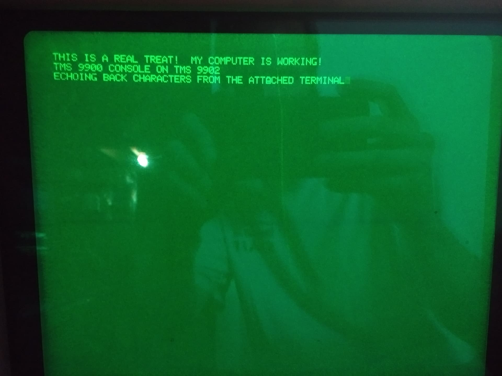
By the next week, the processor booted and communicated with an external TMS 9902 UART, as memorialized by this photo of a Tektronix 4010 graphics terminal that I was using as its console:
The fragility of the design, however, had grown even more significantly, with a second floating breadboard holding the interrupt controller and UART and providing the CRU (serial peripheral bus) decoding logic. Let’s call this system the TIC Mk 0.
By this point, I was developing a boot monitor for the machine (there is a TI monitor called TIBUG available as scanned sources and an OCR’d version from at least one place on the 'net, but I am not (yet?) trying to use it), but development was getting frustrating. The computer was very fragile, and frequently I would spend time chasing after loose connections and dislodged probe wires, rather than doing software development. This was a consequence of having never intended to build up a full working computer on these breadboards, but rather letting some idle puttering grow and grow until it booted.
The logic analyzer and digital storage 'scope were both indispensable in getting to this point. I don’t know that I could have done it, without them – or at least that I would have had the patience to do so. I fought a problem with clocking that was eventually identified with an analog oscilloscope, but some memory/bus issues and problems with a faulty TMS 9902 required the logic analyzer and the DSO, respectively. In particular, the faulty TMS 9902 lost me literally days of development; I am a seasoned enough software developer to know that it’s never the existing code, which I extrapolated to the existing hardware. It turns out that when that hardware is several decades old and purchased as pulls from a Chinese scrapper in Shenzhen, it might be the hardware.
I stalled out on this project some time that fall, and stopped working on it; the fragility of the system was just too frustrating, and other retrocomputing projects took up my hobby time. I worked with my PDP-11/34A hardware, re-capped and cleaned up an Osborne 1, toyed with Beagle Bros’ Program Writer and Microsoft CP/M on an Apple ][, and other diversions instead. Why fight flying leads and dislodged I/O lines when I could play with something that worked? However, I a) wanted my workbench space back, and b) wanted to continue proving out some access and bus logic to have a 9900 PC board built that I could use to put together a complete system.
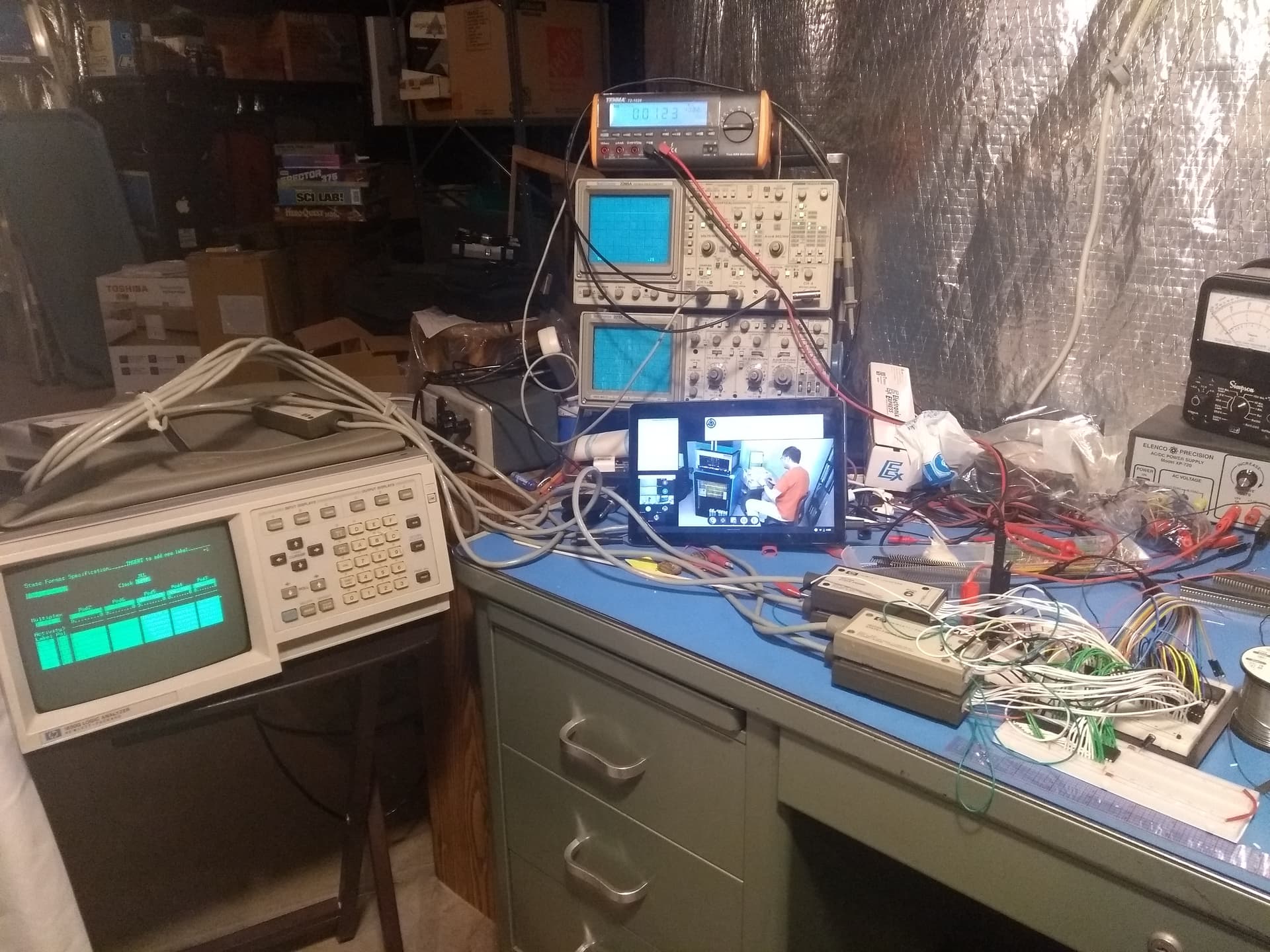
So in the fall of 2021 (about one year later) I gathered up all of the parts that I would need to build a more robust (yet still solderless) implementation, and started reproducing a slightly more complex version of the same system on my desk at work. I am privileged to work in an environment where I can tinker in my down time (though I’m not being paid for that time, but it makes sense to be there anyway, so is that really privileged?), so I swept the usual detritus off my academic workspace and replaced it with vintage components and solderless breadboards. By early 2022, I had a complete replacement plus additional bus buffers and related logic put together in a much more robust configuration and ready to start debugging; we’ll call it the TIC Mk 1.
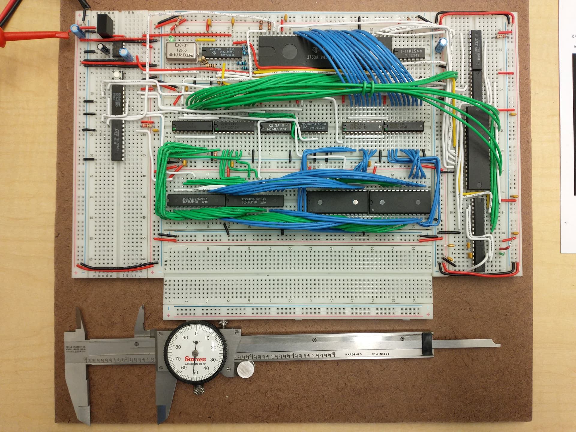
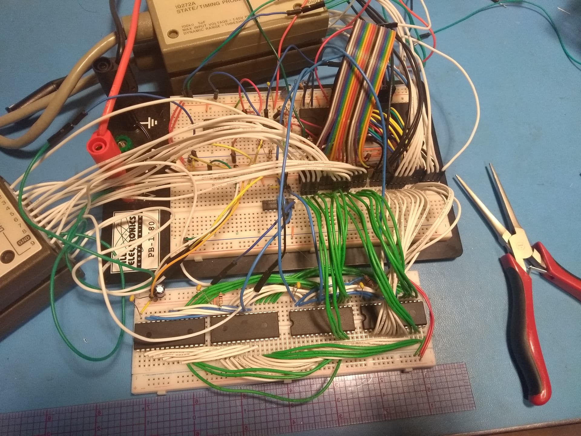
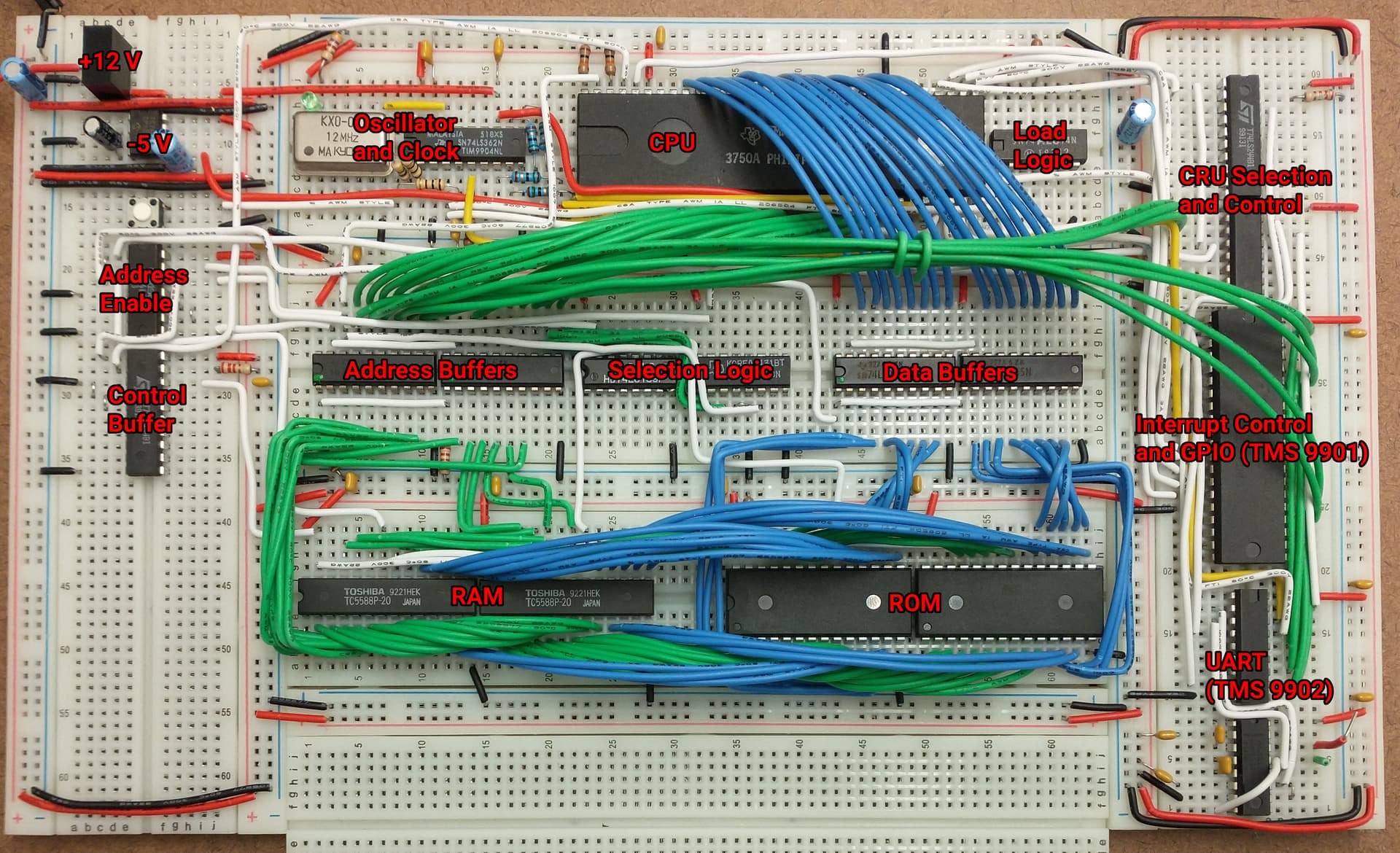
It is immediately obvious that the Mk 1 is a more pleasant environment to work in than the Mk 0 had become! The breadboards are all affixed to the same surface, there is more breadboard space to work in, and the wiring is all measured and cut very neatly to remain mostly out of the way when working and probing. The CPU itself is rather buried, but most other chips can be easily removed and replaced. On this board, green wires are address lines (buffered or unbuffered, but not decoded), blue wires are data lines (buffered or unbuffered), yellow wires are clock, white wires are miscellaneous control signals, and red and black have their usual meanings.
Here is the same board, but with some labels showing where the various parts of the system are laid out:
Note that the entire board runs on a single +5 V supply, and the necessary +12 and -5 V supplies are generated by a switching DC-DC boost converter and a charge pump supply inverter. This is fine for breadboard use and plenty of current is available for both of these purposes, but in the final system (with disk drives and such on the 12 V in particular!) I will use an external multi-voltage power supply to provide these things. It is fortunate that the TMS 9900, while being an NMOS processor that requires a substrate bias, is forgiving about the timing of its positive and negative voltage supply provisions, so I do not have to build a staged power supply. Additionally, by using static RAM, I have eliminated the necessity for a negative supply for (period) DRAM chips and the associated timings for that purpose.
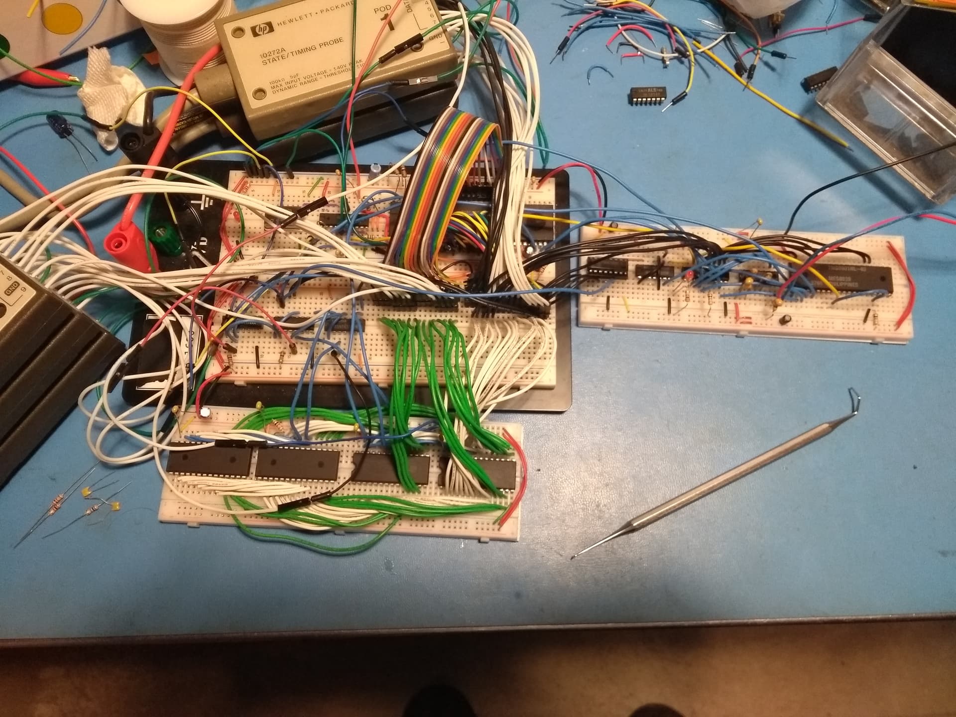
This, of course, did not boot. I wound up having to haul my logic analyzer in to work and hook up the oscilloscope that normally resides on top of a cabinet, and soon the patient looked like this:

That is obviously decidedly less pleasant to work on, but it quickly gave me some useful (though puzzling) information: The processor was doing something that was not entirely unreasonable, it just wasn’t a normal boot sequence. This gave me some confidence that at least the supplies and clocks were doing something (it turns out the latter was a problem), but clearly something was not correct.
The TMS 9900 is a bit of a strange beast in that it loads address 0000h and 0002h when power is applied, and it gets its workspace pointer (the location in RAM where it will store its general purpose register file) and the starting PC value from those locations, but it also uses addresses 0000h through 0100h for interrupt and extended operation (think software interrupt) vectors, which, on a system with a general purpose operating system, almost certainly need to be in RAM. Contrast this to the 6502, which uses a zero page at 0000h through 0100h that usually must be in RAM, but loads its boot vector from FFFEh and FFFFh. This allows RAM to be located at address zero, and ROM the top of memory space. For the 9900, you almost need both RAM and ROM at address zero! The TIC Mk 0 (my first floating breadboard design) used a latch to redirect the ROM bank to the bottom of memory until the processor loads its first instruction, at which point it was shoved to the top of memory and RAM was addressed at address zero. However, the 9900 also has a LOAD line which, when brought low, causes the processor to load a workspace pointer and PC from addresses FFFCh and FFFEh; much more convenient! The Mk 1 is configured to latch LOAD low until the processor fetches its first instruction, and RAM is always low in memory while ROM is always high in memory.
All of this is to say that what I should have seen was a fetches for 0000h and 0002h, then fetches for FFFCh and FFFEh, then the instruction acquisition line (IAQ) going high and the processor loading the first instruction. Instead, I saw this:
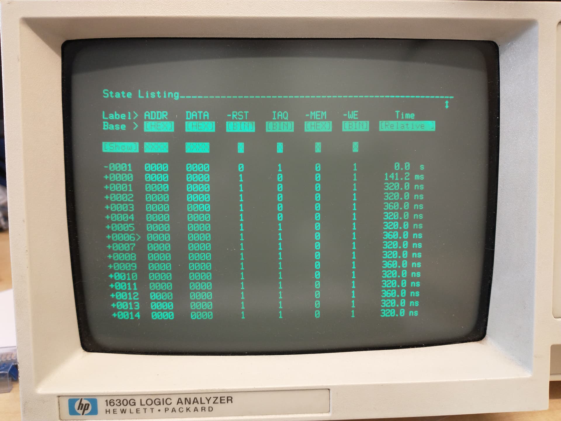
The LOAD line is not visible here, but it was zero from reset until IAQ went high, just as expected. However, the processor was asserting address zero on every single clock cycle! Memory enable (labeled -MEM here) was correct, but the address and data being fetched were always 0000h. Since RAM is at 0000h, the data could reasonably be nearly anything, but we should at least see a fetch for 0000h followed by 0002h, and we do not. There is certainly no attempt to access FFFCh and FFFFh, and it appears to begin executing immediately at the loaded PC of 0000h! Something is definitely fishy.
Remember, way back in the discussion of the Mk 1, when I said that I had to use an oscilloscope to debug a clocking problem? At some point the back of my brain started to tickle on that issue, and I remembered having seen a similar trace in the past. That caused me to put the four phases of the +12 V TMS 9900 clock on the 'scope, where I found this:
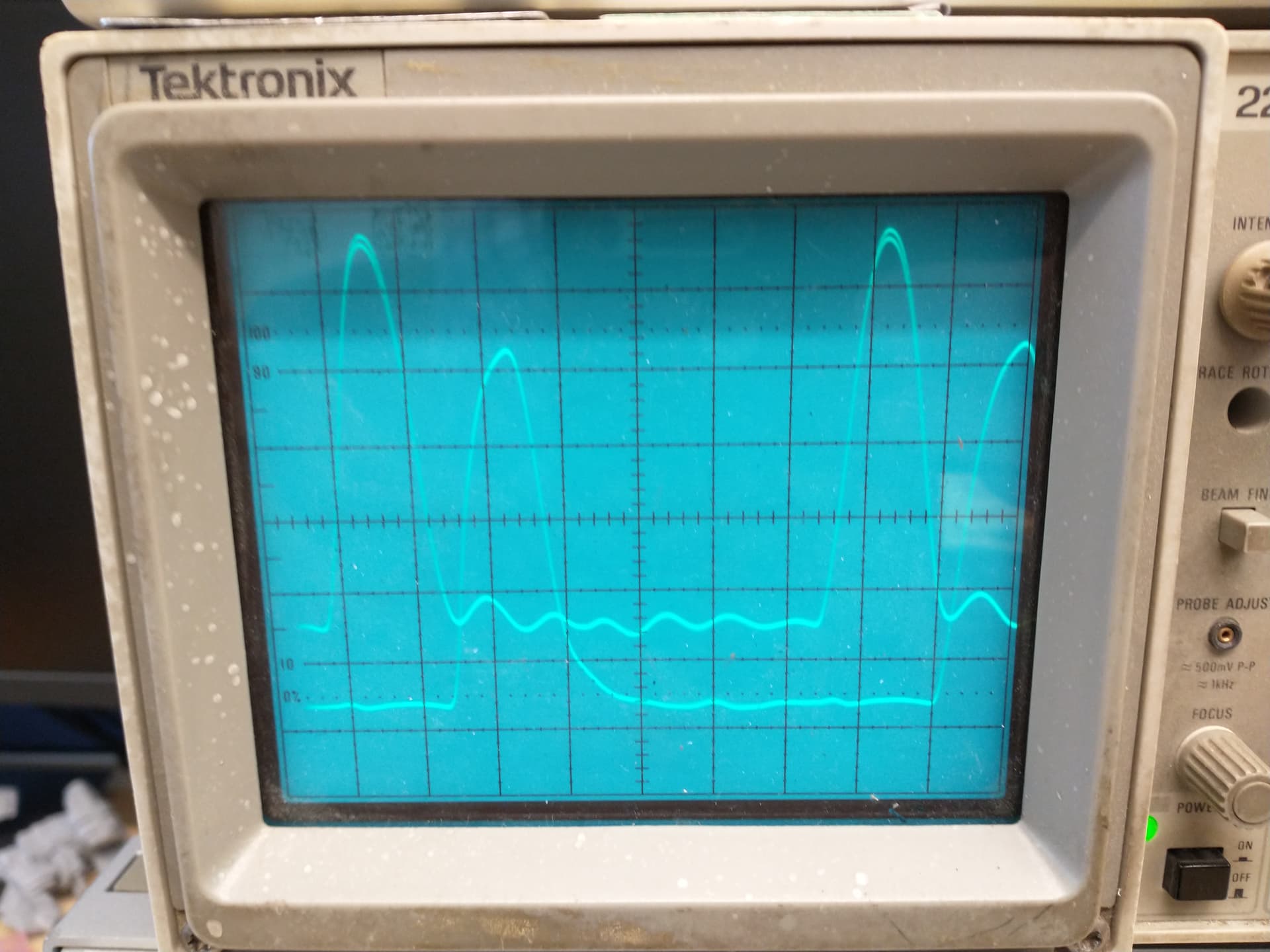
The lower trace in this image is ϕ1, and the upper trace is supposed to be ϕ3, of a four-phase clock where each phase should be 90 degrees from the previous. Note, however, that ϕ3 is immediately leading ϕ1 (270 degrees), while it should be at 180 degrees! I had crossed ϕ3 and ϕ4, which was (apparently) breaking address setup!
Take a look at the pinout of the 64-pin TMS 9900 to see how this might happen:
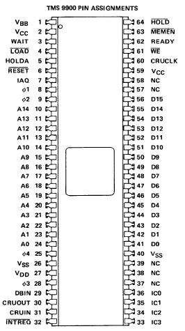
Note that the linear order of the four phases down the side of the chip is … ϕ1, ϕ2, ϕ4, ϕ3! I wired them in 1-2-3-4 order, when they should have been 1-2-4-3. After fixing that, a few minor wiring and logic bugs were uncovered by careful inspection, and unreliable attempts to boot were identified.
The most recent bug to fall (just before leaving the office on Friday of this week) was a high-impedance connection between two breadboard grounds, causing one of the logic chips’ low states to rise over 1 V from the perspective of other chips, which was into the linear region of the IC and causing havoc with signaling. After fixing that, the expected fetches to 0000h, 0002h, FFFCh and then FFFEh showed up on the logic analyzer.
I have high hopes that the Mk 1 will achieve UART communication early this coming week, and that additional software and hardware development can continue in earnest. The purpose of the Mk 1 on a breadboard is to prove out memory and bus management designs in a flexible fashion, so that I can lay out a PCB that will serve as a suitable development platform for an extended period of time (both because it will be more reliable than the solderless breadboard design, and because it will have had most of its kinks worked out before it was etched!). The ultimate goal of the system is to provide: a video console (80 characters) with keyboard, serial I/O, mass storage (both floppy and hard disk, possibly IDE or ATAPI), FM synthesized sound, and the other trappings of a mid-1980s computer. (The TMS 9900 dates from the mid-1970s, but my desire for things like 80 column video and reasonable FM sound pushes my parts collection to the mid 1980s.) Hardware like the video console, disk controllers, and sound device will ideally be provided through cards in a slot architecture. (If I wanted to keep it real with the TMS 9900, I might provide only a single slot, and make them daisy chain!)
I hope to provide additional updates on this journey; I wish I had started this thread a year and a half ago when the project began, and I anticipate additional multi-month stalls as real life interferes with hobby life, but seeing others’ journeys in homebrewing has inspired me to take on this project, so I want to give back some of the story and information. I’ll try to update my TMS 9900 thread with more CPU and architectural information as I go along, as well.