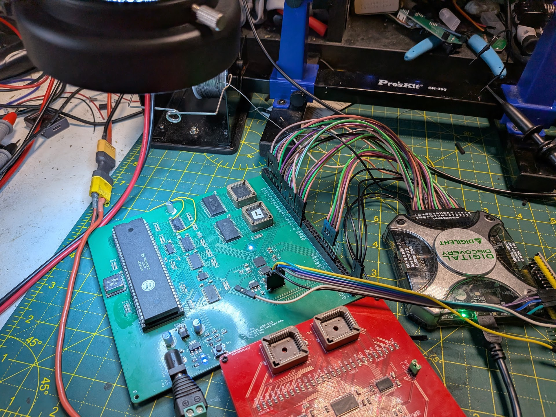
So I wanted to build a computer with a 68010. I have ambitions to create my own virtual memory MMU, hence 68010 and not 68000. I considered the 5V CPLD route, but decided it was not for me. I dont want to fight with accent proprietary software, dongles etc.
So I made my 68010 LVCMOS compliant. 72 channels of level shifters (not all used) and it runs perfectly fine with 3v3 ROM and RAM with a 3v3 FPGA doing the bus decode/glue/dtack etc. Even HALT and RESET bidirectional open drains cross the boundary. Although I split them for sanity into HALT/HALT_ASSERT etc.
Zero wait states on RAM read. 1 wait state on RAM writes. 1 and 2 for the ROM. (Yes the ROM is writable by the CPU!) This is actually the cost of the transceivers OE delaying signals and FPGA clock domain crossing delays. Technically… you would probably get away with 0 wait states for RAM read and write, but for stability and care-free I sacrificed one wait state.
It’s only the start of the fusion.